Silicon optoelectronic device

a technology of optoelectronic devices and silicon materials, applied in non-linear optics, instruments, optical elements, etc., can solve problems such as irregular edges, degraded performance of optical device structures such as optical waveguides, and use of complex and often costly operations

Inactive Publication Date: 2005-09-29
HONEYWELL INT INC
View PDF98 Cites 27 Cited by
  • Summary
  • Abstract
  • Description
  • Claims
  • Application Information

AI Technical Summary

Problems solved by technology

Unfortunately, modern silicon etch systems and processes are optimized so as to prepare vertical features that closely match the dimensions of the masking film.
Such vertical features are efficient and necessary for fabricating poly-silicon gates for advanced microelectronics, but the sharp edges of the vertical features can degrade performance in optical device structures such as optical waveguides.
Also, patterning using these silicon etch systems and processes can contribute to irregular edges, especially when applied to polycrystalline films.
Such devices have typically been assembled in boards and modules from separate optical and electrical components that can include wave guides, diode sources and detectors, drivers, and amplifiers, using complex and often costly operations.
Deposited films with these properties do not, however, satisfy the requirements of electronic device gate electrodes.
Because such a film must be maintained free of impurities and must be protected from conductive layers during the fabrication of the optical device, this film does not provide the necessary work function for efficient surface electronic device construction and does not allow for self-aligned implantation or silicidation.

Method used


Image

  • Silicon optoelectronic device
  • Silicon optoelectronic device
  • Silicon optoelectronic device

Examples


Embodiment Construction

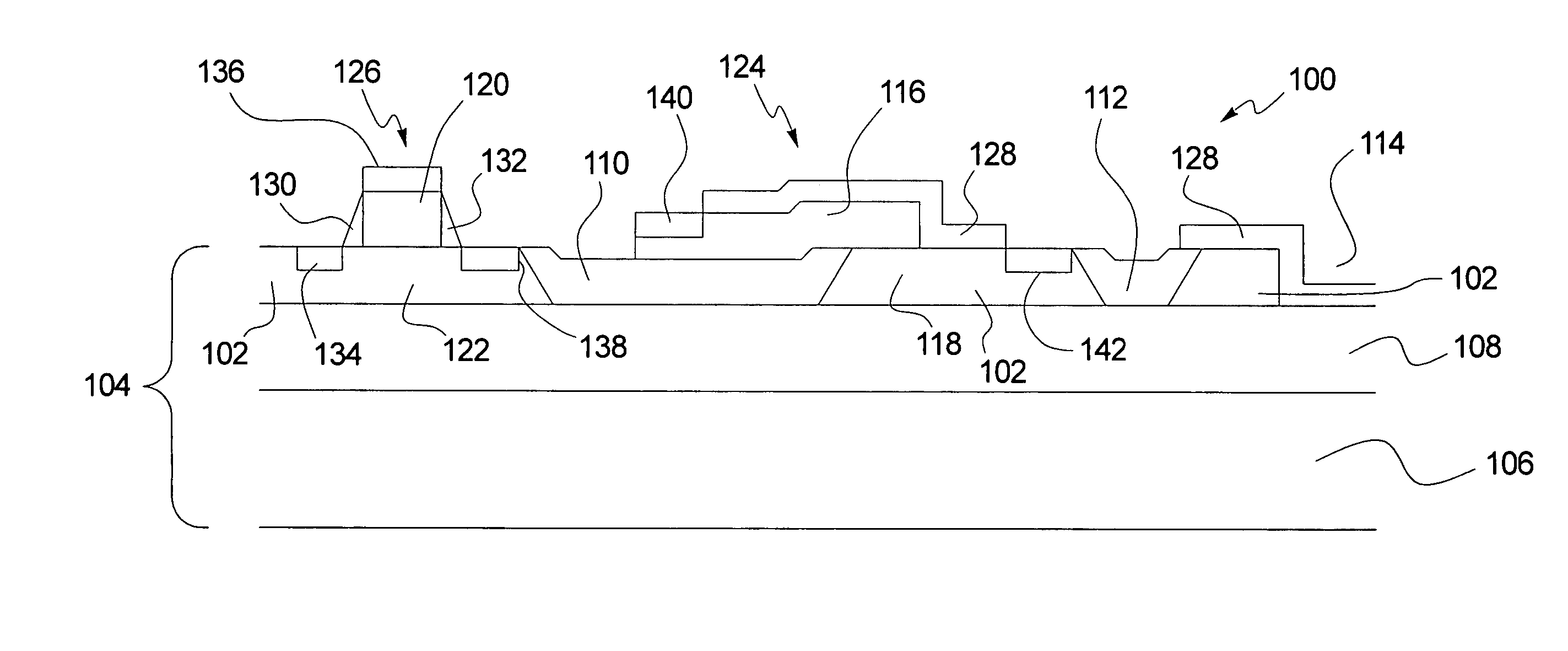
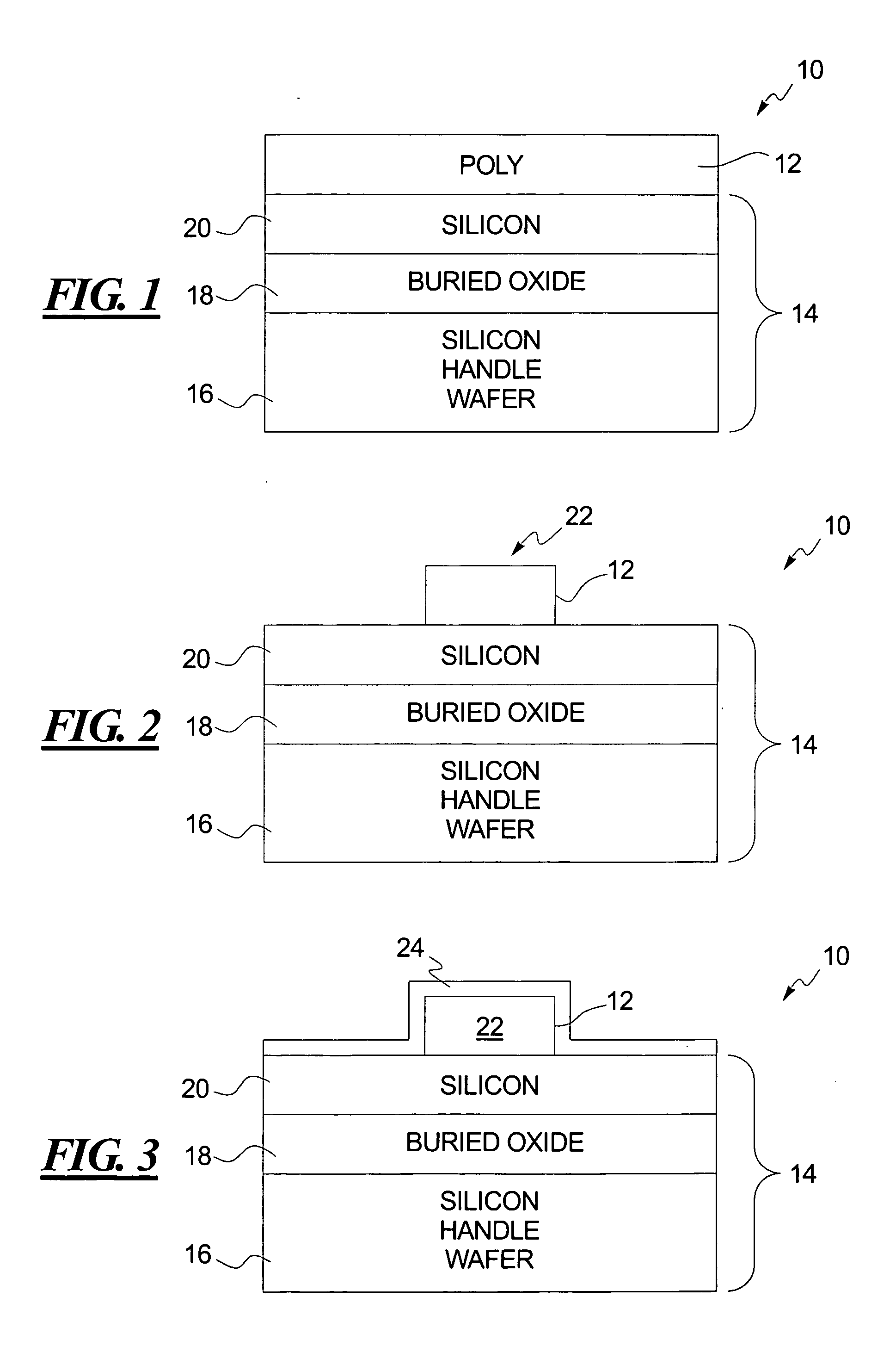
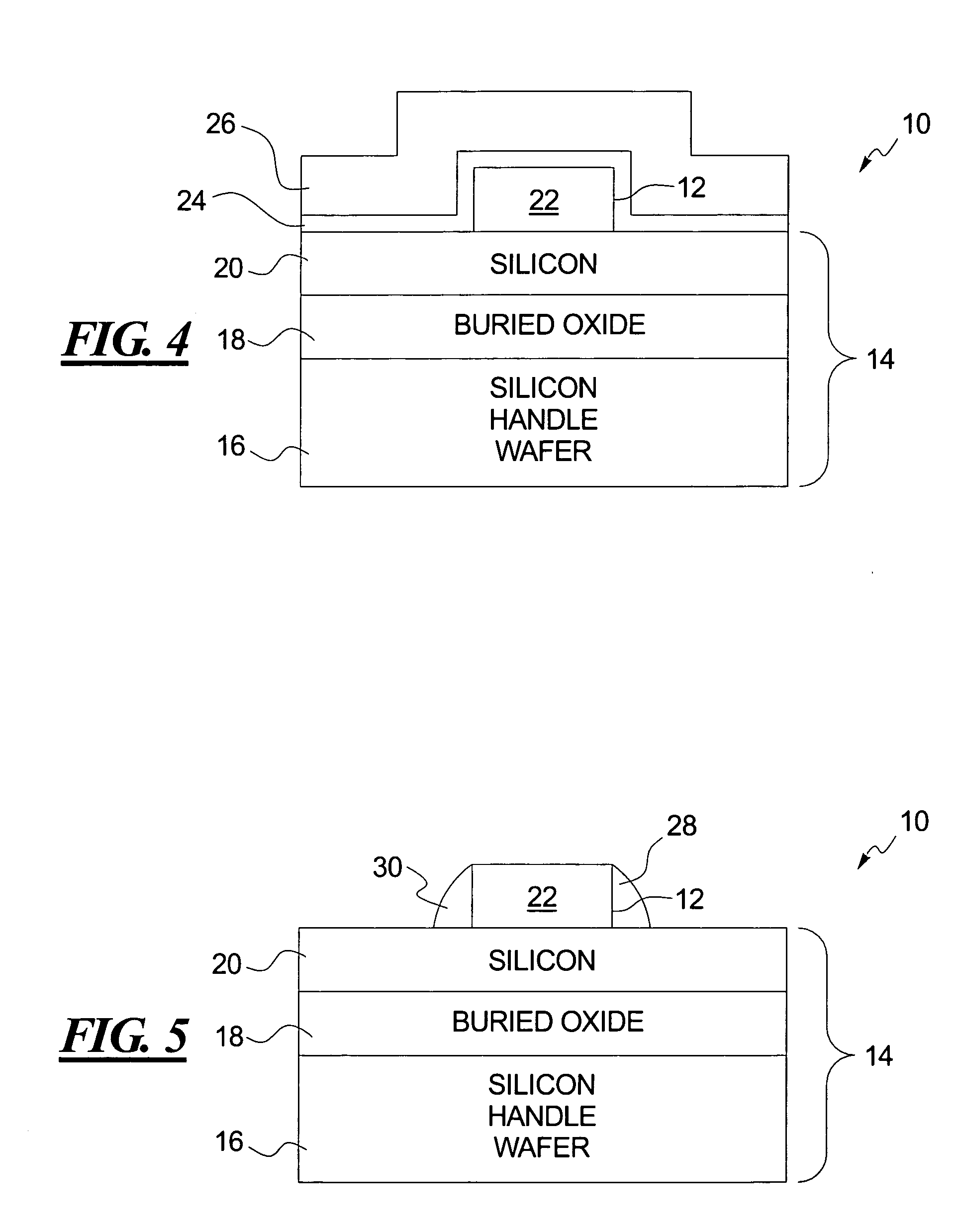
[0023] As shown in FIG. 1, a composite optical device 10 is fabricated by first depositing a poly-silicon layer 12 on a SOI structure 14. If desired, a thin dielectric may be provided between the poly-silicon layer 12 and the SOI structure 14 to help confine dopants and to facilitate poly patterning. This dielectric may be a gate oxide and may have a thickness of 30-100 Å. The poly-silicon layer 12 is preferably, although not necessarily, as crystalline as possible to minimize losses and is indexed-matched to the SOI structure 14 to allow uniform expansion of a light beam into the poly-silicon layer 12 from the SOI structure 14.

[0024] As is typical, the SOI structure 14 includes a silicon handle wafer 16, a buried oxide layer 18 formed over the silicon handle wafer 16, and a silicon layer 20 formed over the buried oxide layer 18. The silicon layer 20, for example, may be formed from single crystal silicon. Also, the thickness of the poly-silicon layer 12, for example, may be on the...


PUM

PropertyMeasurementUnit
thickaaaaaaaaaa
thickaaaaaaaaaa
thicknessesaaaaaaaaaa

Abstract

An optoelectronic integrated circuit is fabricated by forming isolation trenches in a SOI structure to form at least first and second areas of silicon, by forming a first silicon island over the first silicon area during a first silicon forming step such that the first silicon island forms at least a portion of an optical device, by forming a second silicon island over the second silicon area during a second silicon forming step such that the first and second silicon forming steps are separate silicon forming steps, and by processing at least the second silicon area to form an electronic device with the second silicon island.

Description

RELATED APPLICATIONS [0001] The present application contains subject matter similar to the subject matter contained in application Ser. No. 10 / 755,212 filed on Jan. 12, 2004.TECHNICAL FIELD OF THE INVENTION [0002] The present invention relates to optoelectronic devices that combine one or more optical devices and one or more electronic devices on a common semiconductor substrate such as a SOI structure. BACKGROUND OF THE INVENTION [0003] Optical devices such as optical waveguides, optical phase modulators, lenses, etc. can be fabricated in Silicon-on-Insulator (SOI) films in configurations that are compatible with integrated circuit structures. One promising implementation, which has been described elsewhere, involves the use of a single crystal SOI film and the formation of a thin poly-silicon upper layer deposited on the SOI film. In this implementation, the thin poly-silicon upper layer is patterned to form a light guiding element or patterned with the SOI film to form SOI / poly c...

Claims


Application Information

Patent Timeline
Patent Type & Authority Applications(United States)
IPC IPC(8): G02B6/12G02B6/136G02B6/42G02F1/01G02F1/025H01L21/84H01L27/13H01L31/12
CPCG02B6/136H01L31/12G02F2202/104G02F1/011
Inventor KEYSER, THOMAS R.
Owner HONEYWELL INT INC
Why Eureka
Try Eureka