Image exposure device and laser exposure device applied thereto

a laser exposure and image technology, applied in semiconductor lasers, printing, instruments, etc., can solve the problems of remarkable degradation, extremely high sensitivity, and blurry characters and blurry images, and achieve the effect of maximizing the diffraction efficiency

Inactive Publication Date: 2005-10-06
FUJIFILM CORP
View PDF8 Cites 135 Cited by
  • Summary
  • Abstract
  • Description
  • Claims
  • Application Information

AI Technical Summary

Benefits of technology

[0038] It is preferable to dispose the semiconductor laser so that the electric field faces a direction substantially orthogonal to an effective diffraction grating surface of the diffraction unit. By making the electric field incident on the diffraction grating surface, diffraction efficiency is maximized. Also, a spatial modulator that is separate from the diffraction unit for diffracting laser light and spatially modulates the intensity of the diffracted light can also be disposed between the semiconductor laser and the photosensitive material.
[0039] Particularly remarkable effects can be obtained when the laser exposure device of the invention is applied to a highly sensitive photosensitive material that is exposed by density gradation, such as a silver halide photosensitive material.

Problems solved by technology

In comparison to electrophotographic methods using photosensitive materials such as photosensitive drums, the blurry pattern 199 becomes a fatal defect (i.e., the photosensitive material reacts due to the stray light) in high-resolution silver halide exposure methods, which have extremely high sensitivity.
However, in continuous-tone photosensitive materials such as those used in silver halide photography, a slight background leads to blurry characters and blurry images and remarkable degradation.
In exposure of silver halide methods, which are characterized by high-resolution images, it is necessary to reduce stray light that is inherent to GaN based semiconductor lasers and exerts an adverse, critical, and fatal impact on an image.
However, there is a problem in that, when a GaN based semiconductor laser is used for the light source in an exposure device, sharpness of the spot contour cannot be obtained due to the unintended stray light even if the beam diameter is reduced by operating the optical system.
Particularly in silver halide methods, in which a continuous-tone high-resolution photographic image is formed by exposing a silver halide photosensitive material that is highly sensitive, lack of sharpness of the spot contour becomes a fatal problem in comparison to electrophotographic methods in which an image is structured by halftone dots.

Method used


Image

  • Image exposure device and laser exposure device applied thereto
  • Image exposure device and laser exposure device applied thereto
  • Image exposure device and laser exposure device applied thereto

Examples


first embodiment

[0076] An example of a first embodiment of the invention will be described in detail below with reference to the drawings. It should be noted that the present embodiment is one in which the invention is applied to a digital laboratory system.

Schematic Description of Overall System

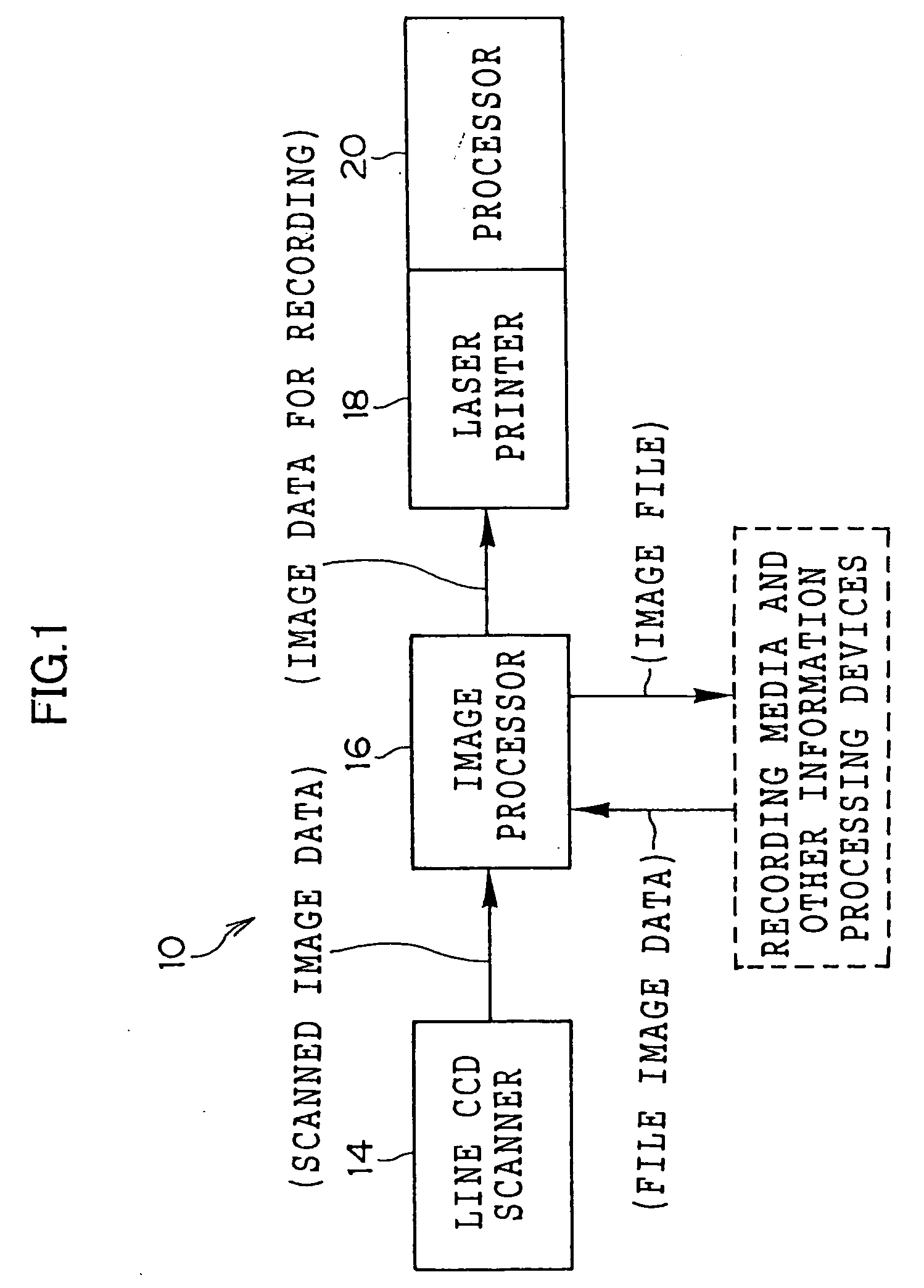
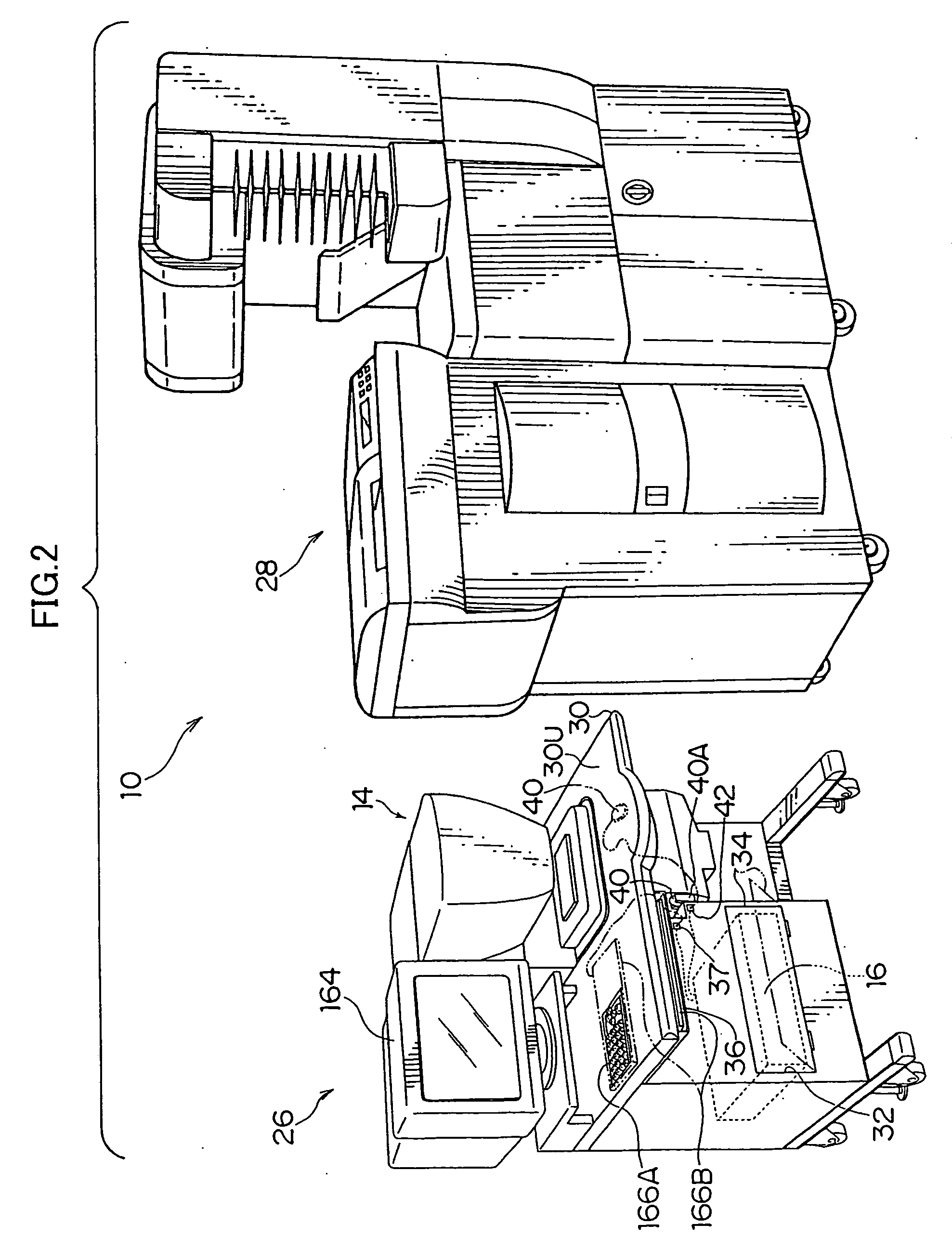
[0077]FIG. 1 shows the schematic structure of a digital laboratory system 10 pertaining to an embodiment of the invention, and FIG. 2 shows the digital laboratory system 10 in perspective view. As shown in FIG. 1, the digital laboratory system 10 comprises a line CCD scanner 14, an image processor 16, a laser printer 18 that serves as an image exposure device, and a processor 20. As shown in FIG. 2, the line CCD scanner 14 and the image processor 16 are integrated as an input section 26, and the laser printer 18 and the processor 20 are integrated as an output section 28.

[0078] The line CCD scanner 14 is for reading a film image (a negative image or a positive image visualized by developing and processin...

second embodiment

[0124] Next, a second embodiment of the invention will be described. Description of structures that are the same as those described in the first embodiment will be omitted.

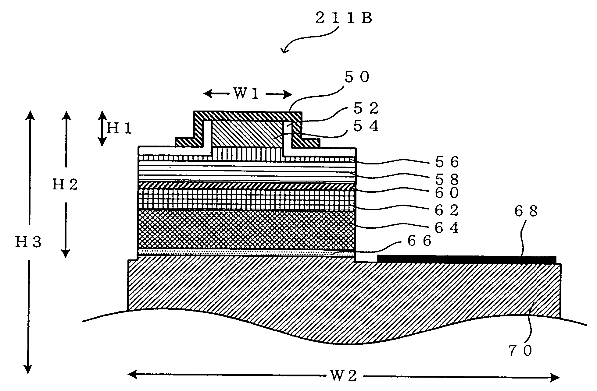
[0125] In the second embodiment of the invention, in contrast to the laser printer in the first embodiment, the collimator lens 213, the limiter 200, and the cylindrical lens 217 are successively disposed at the laser light emission side of the laser light source 211B. Laser light emitted from the laser light source 211B is collimated by the collimator lens 213, and an amount of light that is predetermined in correspondence to the amount of light emitted from the laser light source 211B is limited by the limiter 200. The laser light is irradiated at a position that is substantially the same as the above-described predetermined position on the reflective surface of the polygon mirror 218 and reflected by the polygon mirror 218.

[0126] It is possible to use a light filter (density filter or the like) or a half mirr...

third embodiment

[0141] Next, a third embodiment of the invention will be described. Description of structures that are the same as those described in the first and second embodiments will be omitted.

[0142] The laser printer in the third embodiment of the invention includes the following characteristics that are different from those of the first and second embodiments.

[0143] The collimator lens 213 and the cylindrical lens 217 are successively disposed at the laser light emission side of the laser light source 211R. Laser light emitted from the laser light source 211R is collimated by the collimator lens 213 and irradiated via cylindrical lens 217 at a position that is substantially the same as the above-described predetermined position on the reflective surface of the polygon mirror 218 and reflected by the polygon mirror 218.

[0144] The collimator lens 212 and the acoustooptic modulator (AOM) 214G that serves as an outside modulator are successively disposed at the laser light emission side of t...


PUM


Abstract

When a ratio R between a total angle φ of a widening angle in a median intensity of light of a light source (a GaN based semiconductor laser) and a total angle 2/φ of a widening angle of light defining a numerical aperture NA of a collimator optical system (collimator lens) is defined as R=(sin−1NA)×2/φ, the numerical aperture of the collimator optical system (collimator lens) is set so that 2.0≧R≧0.58. Thus, an image exposure device is provided that can suppress stray light of a light source that emits a large amount of stray light.

Description

BACKGROUND OF THE INVENTION [0001] 1. Field of the Invention [0002] The present invention relates to an image exposure device, particularly an image exposure device that is disposed with a GaN based semiconductor laser, modulates a laser beam, and scan-exposes a recording material such as photosensitive material with the laser beam, and to a laser exposure device applied thereto. [0003] 2. Description of the Related Art [0004] Image exposure devices that scan a recording material with light and expose an image thereon using a light source device that includes an edge emitting LED (a super luminescent diode (SLD) or the like) or a semiconductor laser taking as a structural material AlGaInP, AlGaAs, or InGaAsP of a GaAs substrate shape have been proposed. [0005] In light source devices that use such materials, GaAs, which serves as the substrate with respect to an emission wavelength, is an absorbent material, and light absorbent materials such as InGaAs are also used in opposing elec...

Claims


Application Information

Patent Timeline
Patent Type & Authority Applications(United States)
IPC IPC(8): G03B27/42
CPCG03B27/42
Inventor MATSUMOTO, KENJIHAYAKAWA, TOSHIROMORIMOTO, YOSHINORIKATO, KIICHI
Owner FUJIFILM CORP
Why Eureka
Try Eureka