Supercharge Your Innovation With Domain-Expert AI Agents!

Halogen gettering method for forming field effect transistor (FET) device

a field effect transistor and halogen gettering technology, applied in the direction of semiconductor devices, basic electric elements, electrical equipment, etc., can solve the problems of increasing difficulty in formation and the fact that the field effect transistor devices are not entirely without problems

Inactive Publication Date: 2005-10-06
TAIWAN SEMICON MFG CO LTD
View PDF3 Cites 8 Cited by
  • Summary
  • Abstract
  • Description
  • Claims
  • Application Information

AI Technical Summary

Benefits of technology

The invention provides a method for making a field effect transistor device with enhanced performance. This is achieved by using a thermal oxidizing atmosphere containing a halogen getter material when thermally oxidizing a semiconductor substrate to form a gate dielectric layer. This method results in a more effective field effect transistor device.

Problems solved by technology

While field effect transistor devices are thus common in the semiconductor product fabrication art and often essential for fabricating semiconductor products, field effect transistor devices are nonetheless not entirely without problems.
In that regard, as semiconductor product integration levels have increased and semiconductor device dimensions have decreased, it has become increasingly difficult to form within semiconductor products field effect transistor devices with enhanced performance.

Method used


Image

  • Halogen gettering method for forming field effect transistor (FET) device
  • Halogen gettering method for forming field effect transistor (FET) device
  • Halogen gettering method for forming field effect transistor (FET) device

Examples


example

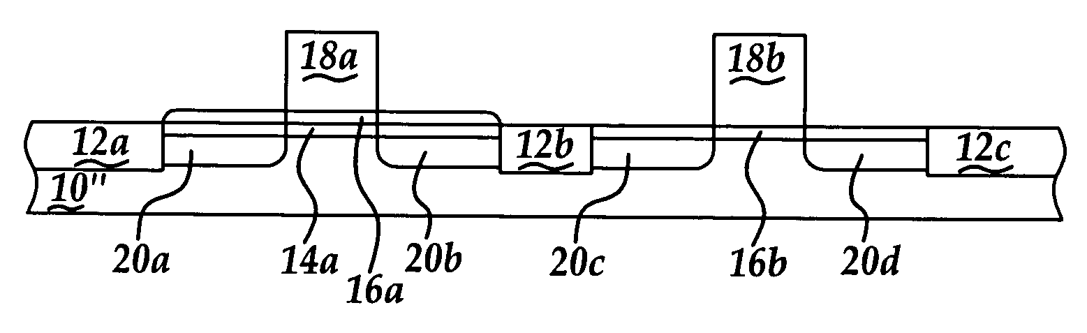
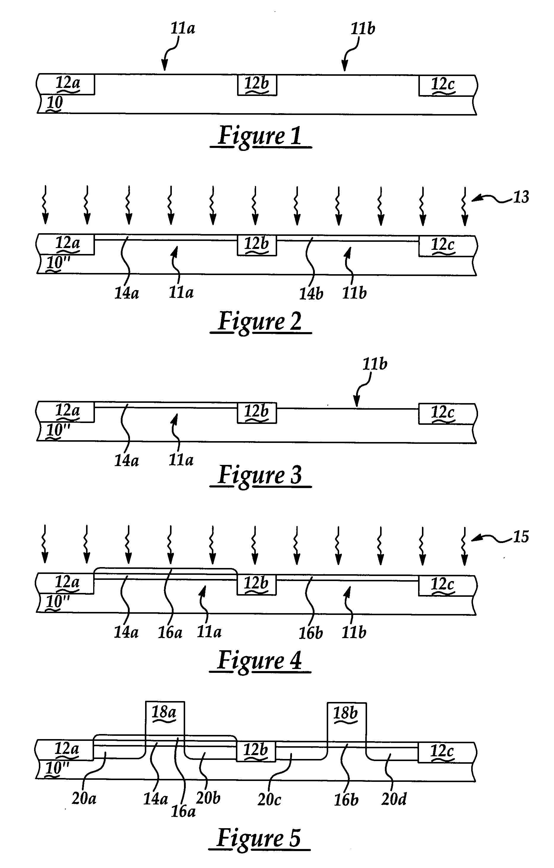
[0046] To illustrate the value of the invention, a semiconductor product having formed therein two field effect transistor devices was fabricated in accord with the preferred embodiment of the invention.

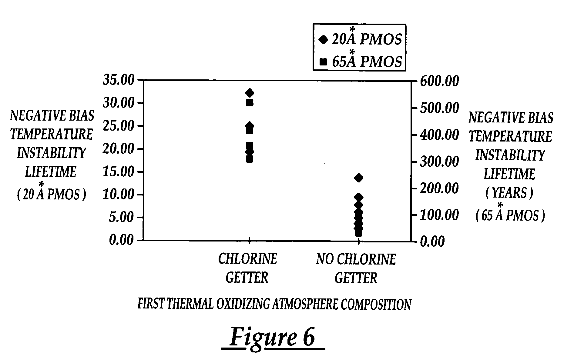
[0047] The semiconductor product comprised a semiconductor substrate having formed thereupon a pair of non-nitrided silicon oxide gate dielectric layers formed employing a first thermal oxidation of a semiconductor substrate within a first thermal oxidizing atmosphere comprising a transdichloroethylene chlorine getter material when thermally oxidizing the semiconductor substrate. The first thermal oxidation method also employed: (1) a reactor chamber pressure of about 760 torr; (2) a thermal oxidation temperature of about 800 degrees centigrade; (3) a dry oxygen oxidant at a flow rate of about 4000 standard cubic centimeters per minute; and (4) a transdichloroethylene flow rate of about 250 standard cubic centimeters per minute. The first thermal oxidation method provided a pair of ...


PUM


Abstract

A thermal oxidation method for forming a gate dielectric layer for use within a field effect transistor device employs a thermal oxidizing atmosphere comprising a halogen getter material. By employing the halogen getter material, the field effect transistor device is formed with enhanced performance, in particular with respect to negative bias temperature instability lifetime.

Description

BACKGROUND OF THE INVENTION [0001] 1. Field of the Invention [0002] The present invention relates generally to methods for forming field effect transistor (FET) devices. More particularly, the present invention relates to methods for forming field effect transistor (FET) devices with enhanced performance. [0003] 2. Description of the Related Art [0004] Common in the semiconductor product fabrication art is the fabrication and use of field effect transistor devices as switching devices within logic semiconductor products, memory semiconductor products and embedded logic and memory semiconductor products. [0005] While field effect transistor devices are thus common in the semiconductor product fabrication art and often essential for fabricating semiconductor products, field effect transistor devices are nonetheless not entirely without problems. [0006] In that regard, as semiconductor product integration levels have increased and semiconductor device dimensions have decreased, it has ...

Claims


Application Information

Patent Timeline
Patent Type & Authority Applications(United States)
IPC IPC(8): H01L21/00H01L21/28H01L21/8234H01L29/51
CPCH01L21/28202H01L29/513H01L21/823462H01L21/28211
Inventor HAO, CHING-CHENCHEN, CHAO-CHISHEN, CHIH-HENGHSIEH, CHI-HSUN
Owner TAIWAN SEMICON MFG CO LTD
Features
  • R&D
  • Intellectual Property
  • Life Sciences
  • Materials
  • Tech Scout
  • Unparalleled Data Quality
  • Higher Quality Content
  • 60% Fewer Hallucinations
Learn More