Optical recording medium
- Summary
- Abstract
- Description
- Claims
- Application Information
AI Technical Summary
Benefits of technology
Problems solved by technology
Method used
Image
Examples
example 1
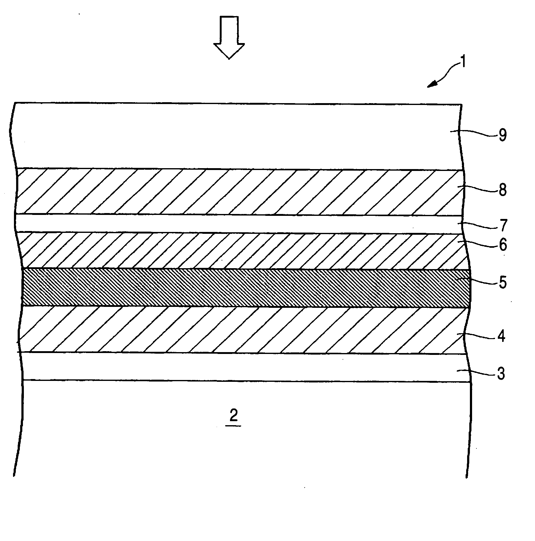
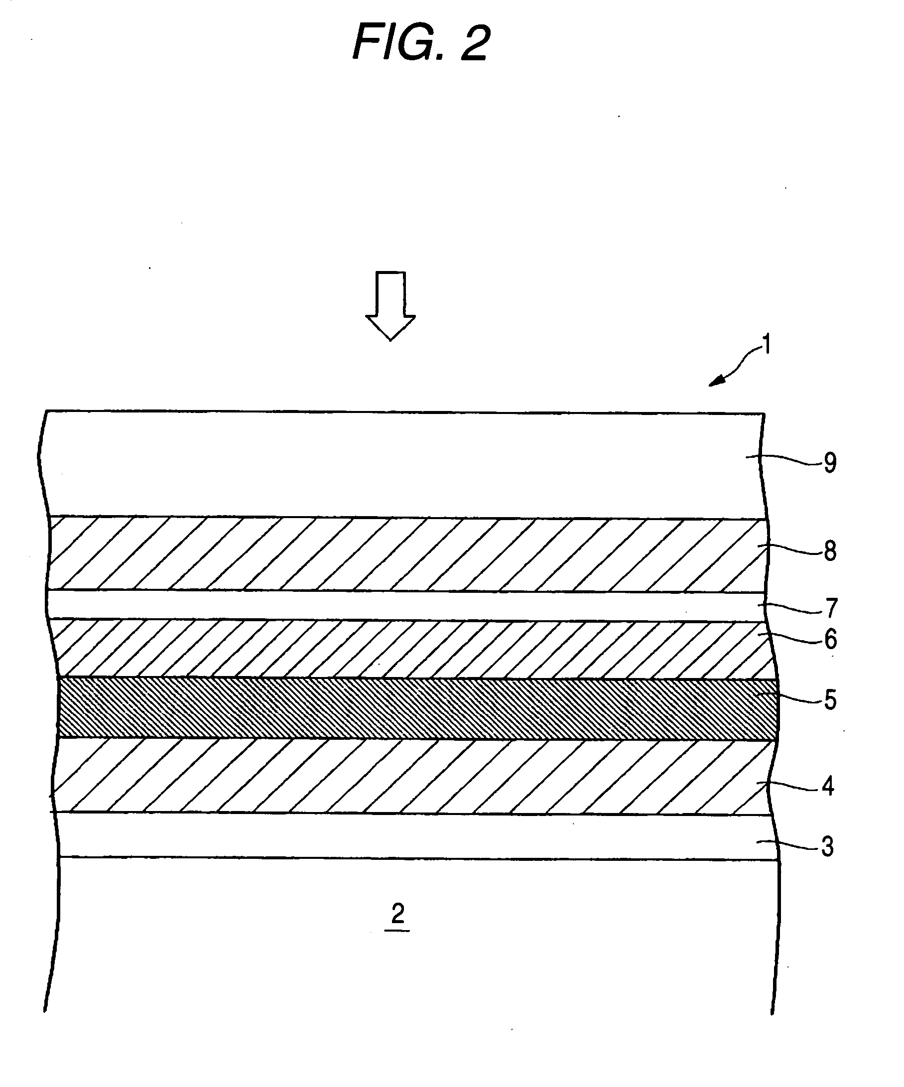
[0175] A polycarbonate substrate of 1.1 mm in thickness and 120 mm in diameter was set to a sputtering apparatus, and a reflecting layer of 20 nm in thickness is formed on the polycarbonate substrate by the sputtering method using a Pt target.
[0176] Subsequently, a third dielectric layer of 100 nm in thickness was formed by the sputtering method with a mixture of ZnS and SiO2 as a target. The target mixture of ZnS and SiO2 used here was a target in which the mol ratio between ZnS and SiO2 was 80:20.
[0177] Subsequently, a light absorbing layer of 20 nm in thickness was formed on the surface of the third dielectric layer by the sputtering method with the Sb and Sn as the target. The composition of the light absorbing layer was Sb41.5Sn58.5 in atomic ratio.
[0178] Subsequently, by using the target composed of the mixture of ZnS and SiO2, a second dielectric layer of 60 nm in thickness was formed on the surface of the light-absorbing layer by the sputtering method. The target mixture ...
example 2
[0196] A light absorbing layer having the same composition as the light absorbing layer of the sample #1 and of 250 nm in thickness was formed on the surface of a polycarbonate substrate of 1.2 mm in thickness to form a sample #1-1.
[0197] Then, a light absorbing layer having the same composition as the light absorbing layer of the sample #2 and of 250 nm in thickness was formed on the surface of a polycarbonate substrate of 1.2 mm in thickness to form a sample #2-1.
[0198] Subsequently, using the X-ray diffracting device “ATX-G” (name of product) from Rigaku Corporation, the crystalline states of the light absorbing layers of the sample #1-1 and the sample #2-1 were analyzed. For analyzing the crystalline states of the light absorbing layers, Cu was used as a target, and the tube pressure was set to 50 kV, and the tube current was set to 300 mA.
[0199] As a result of analysis, it was found that the light absorbing layers are entirely crystalline material in the samples #1-1 and #2-...
example 3
[0203] Except for the point that the composition of the light absorbing layer was set to Sb90.8Sn9.2 in atomic ratio, a sample #3 was manufactured in the same manner as the sample #1.
[0204] Subsequently, except for the point that the composition of the light absorbing layer was changed as shown in Table 1, samples #4 and #11, and comparative samples #2 and #3 are manufactured in the same manner as the sample #3.
TABLE 1Content (atomic %)SbSnSample #479.520.5Sample #575.724.3Sample #664.335.7Sample #752.947.1Sample #841.558.5Sample #930.269.8Sample #1015.085.0Sample #1111.188.9Comparative Sample #21000Comparative Sample #30100
[0205] Subsequently, the sample #3 and the comparative sample #3 are set in sequence in the above-described optical recording medium verification device, recording mark rows including recording marks of 75 nm and blank areas of 75 nm were formed on the recording layers of the sample #3 and the comparative sample #3, and data were recorded. For recording data o...
PUM
| Property | Measurement | Unit |
|---|---|---|
| Percent by atom | aaaaa | aaaaa |
| Percent by atom | aaaaa | aaaaa |
| Percent by atom | aaaaa | aaaaa |
Abstract
Description
Claims
Application Information


