Electrophotographic photoconductor and image formation method, image formation apparatus, and process cartridge for image formation apparatus using the electrophotographic photoconductor

a photoconductor and electrophotography technology, applied in the direction of electrographic process, instruments, corona discharge, etc., can solve the problems of reducing the photosensitivity, degrading the electric characteristic, and the organic photoconductor, and achieve excellent smoothness, good electric characteristic, and high abrasive resistance

Inactive Publication Date: 2005-10-06
RICOH KK
View PDF38 Cites 72 Cited by
  • Summary
  • Abstract
  • Description
  • Claims
  • Application Information

AI Technical Summary

Benefits of technology

[0010] One of the objects of the present invention is to provide an electrophotographic photoconductor which has high abrasive resistance, a surface with excell

Problems solved by technology

From this viewpoint, since a surface layer of the organic photoconductor is based on a low-molecular-weight charge transportation material and an inactive polymer, the organic photoconductor is generally soft, and, therefore, has a disadvantage of abrasion caused easily by mechanical load from a development system or a cleaning system, when the organic photoconductor is used repeatedly in an electrophotographic process.
Such abrasion of the photoconductor lowers the photosensitivity and degrades electric characteristics such as the charging property, so as to cause the lowering in image density and improper imaging such as background contamination.
Also, the damage caused by local abrasion results in insufficient cleaning, and, therefore, leads to an image with stripe-like contamination.
ed. Among these techniques, (1) the use of a curable binder tends to reduce image density caused by the elevation of a residual electric potential due to a low compatibility with a charge transportation material and impurities such as a polymerization initiator and an unreacted resi
due. Also, (2) the use of a polymeric charge transportation material can improve abrasive resistance to some extent, but have not sufficiently satisfied durability required for an organic photocondu
ctor. Further, since the polymerization and purification of the material for a polymeric charge transportation material are difficult, it is difficult to obtain a polymeric charge transportation material with high purity and the electric characteristics of the polymeric charge transportation material tends to be uns
table. Moreover, a problem such that coating liquid for it has high viscosity in the manufacturing process may
density. Also, when the irregular

Method used


Image

  • Electrophotographic photoconductor and image formation method, image formation apparatus, and process cartridge for image formation apparatus using the electrophotographic photoconductor
  • Electrophotographic photoconductor and image formation method, image formation apparatus, and process cartridge for image formation apparatus using the electrophotographic photoconductor
  • Electrophotographic photoconductor and image formation method, image formation apparatus, and process cartridge for image formation apparatus using the electrophotographic photoconductor

Examples


example 1

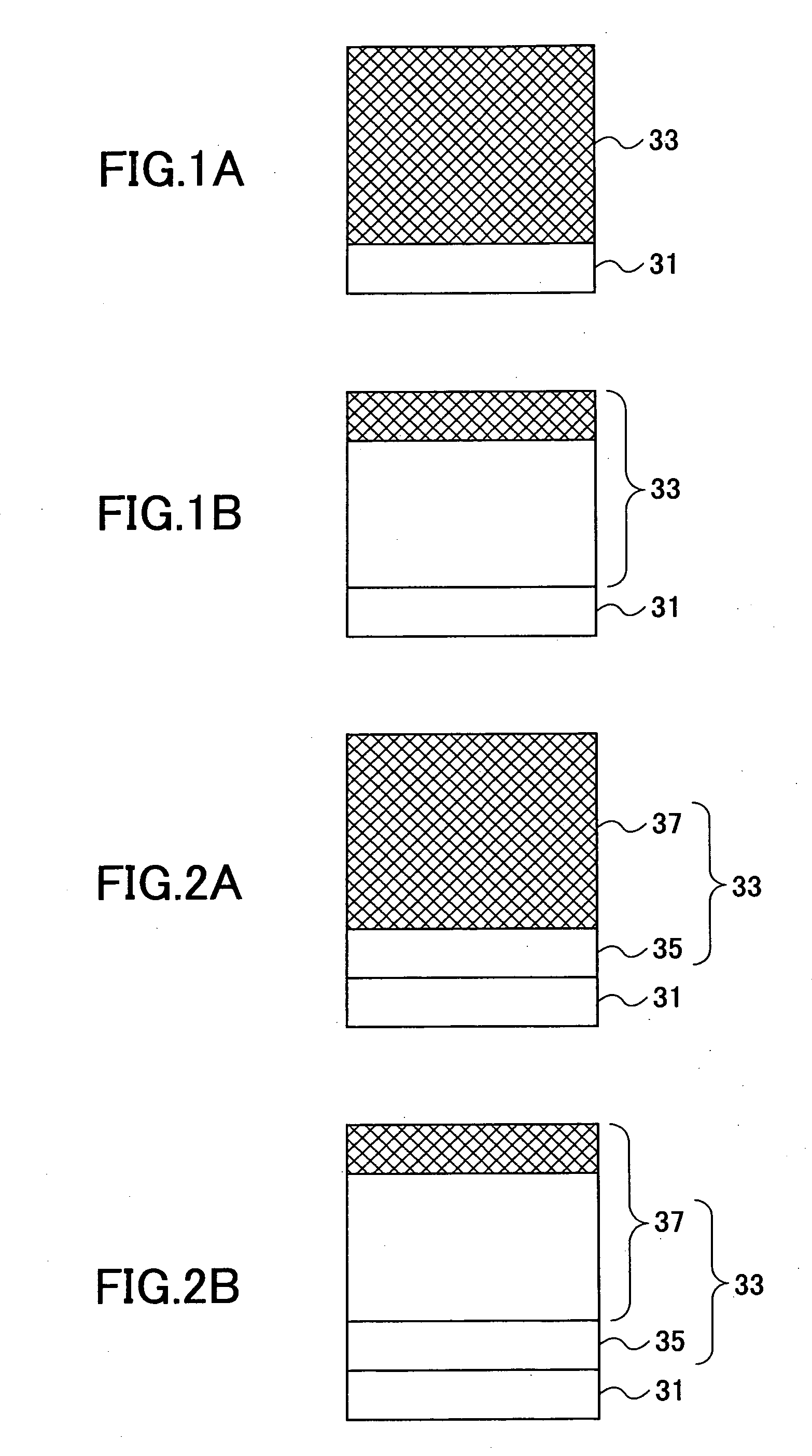
[0231] Coating liquid for underlying layer, coating liquid for charge generation layer, and coating liquid for charge transportation layer, which had the following compositions, were applied on an aluminum cylinder with φ 30 mm in order and dried so as to form an underlying layer with 3.5 μm, a charge generation layer with 0.2 μm, and a charge transportation layer with 18 μm. Then, coating liquid for crosslinked surface layer that had the following composition was spray-coated on the charge transportation layer and light irradiation was performed by using a metal halide lamp 120 W / cm under the conditions of an illuminance of 350 mW / cm2, and an irradiation time of 15 seconds. Further, the drying was performed at 130° C. for 20 minutes so as to form a crosslinked surface layer with 6 μm. Thus, an electrophotographic photoconductor according to the present invention was obtained.

[0232] [Coating Liquid for Underlying Layer][0233] Alkyd resin: 6 parts [0234] (Beckosol 1307-60-EL produce...

example 2

[0265] An electrophotographic photoconductor was manufactured similar to example 1 except that the photo-polymerization initiator in example 1 was changed to an acylphosphine oxide compound having the following structure. [0266] Photo-polymerization initiator: 0.6 parts [0267] Lucirin TPO (produced by BASF)

[0268] (Acylphosphine Oxide Compound) [0269] 2,4,6-trimethylbenzoyl-diphenylphosphine oxide

example 3

[0270] An electrophotographic photoconductor was manufactured similar to example 1 except that the photo-polymerization initiator in example 1 was changed to a mixture of photo-polymerization initiators that contain an acylphosphine oxide compound having the following structure. [0271] Mixed photo-polymerization initiators: 0.6 parts [0272] Irgacure-1700 (produced by Ciba Specialty Chemicals)

[0273] (Acylphosphine Oxide Compound) [0274] bis(2,6-dimethoxybenzoyl)-2,4,4,-trimethylpentylphosphine oxide: 25%

[0275] (Another Photo-Polymerization Initiator) [0276] 2-hydroxy-2-methyl-1-phenylpropane-1-one: 75%


PUM

PropertyMeasurementUnit
Volumeaaaaaaaaaa
Fractionaaaaaaaaaa
Fractionaaaaaaaaaa

Abstract

An electrophotographic photoconductor having at least a photoconductive layer on an electrically conductive support, wherein a surface layer of the photoconductive layer is a crosslinked layer obtainable by curing at least a three or more-functional radical-polymerizable monomer having no charge transporting structure and a charge transportation compound having a radical-polymerizable functional group by using an acylphosphine oxide compound as a photo-polymerization initiator under light energy irradiation.

Description

BACKGROUND OF THE INVENTION [0001] 1. Field of the Invention [0002] The present invention relates to an electrophotographic photoconductor which has high durability and can realize high quality image formation for a long period, using a photoconductive layer with high abrasive resistance, a smooth surface, and good electrical characteristics. Also, the present invention relates to an image formation method, an image formation apparatus and a process cartridge for image formation apparatus using the aforementioned photoconductor with high performance and a long operating life. [0003] 2. Description of the Related Art [0004] Recently, an organic photoconductor (OPC) is frequently used in a copying machine, a facsimile machine, a laser printer, and a complex machine thereof, due to good performance and various advantages of it, instead of an inorganic photoconductor. As the reasons, for example, (1) excellent optical properties such as a wider wavelength range for light absorption and ...

Claims


Application Information

Patent Timeline
IPC IPC(8): G03G5/043G03G5/047G03G5/147G03G5/05G03G5/06G03G5/07
CPCG03G5/0542G03G5/0546G03G5/0592G03G5/0596G03G5/0601G03G5/0605G03G5/0609G03G5/062G03G5/071G03G5/14708G03G5/1473G03G5/14734G03G5/14791G03G5/14795G03G5/072G03G5/0745G03G5/0732G03G5/074
Inventor SUZUKI, TETSUROTAMURA, HIROSHIIKUNO, HIROSHIYANAGAWA, YOSHIKINAGAI, KAZUKIYOLI, HONGGUO
Owner RICOH KK
Why Eureka
Try Eureka