Top-emission organic electroluminescent display and method of fabricating the same
- Summary
- Abstract
- Description
- Claims
- Application Information
AI Technical Summary
Benefits of technology
Problems solved by technology
Method used
Image
Examples
example
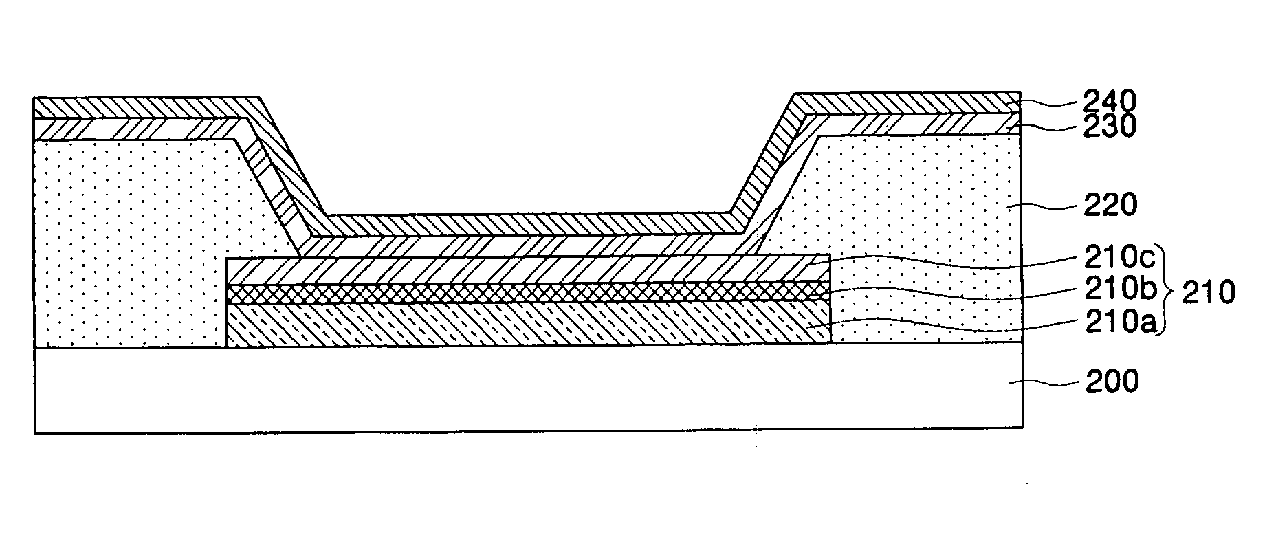
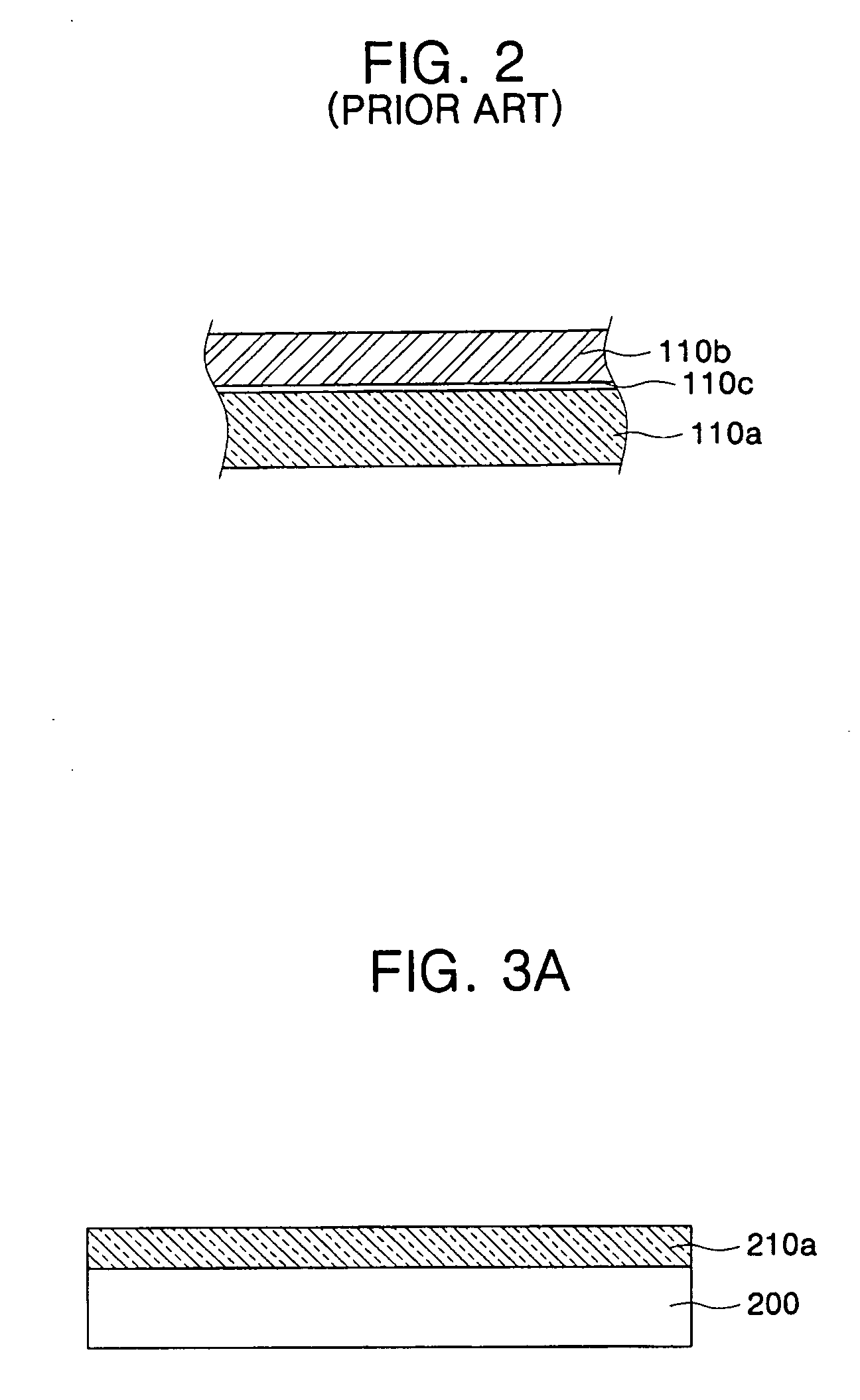
[0054] To fabricate a top-emission organic electroluminescent display according to the exemplary embodiment of the present invention, after sputtering of Al and Nd was performed onto a glass substrate to form an Al—Nd reflective layer having a thickness of about 1000 Å, sputtering of Al and α-Si was continuously performed at a temperature of about 200° C. to form an aluminum-silicide layer having a thickness of about 150 Å. Next, ITO as a transparent electrode material was vacuum deposited to a thickness of about 125 Å on the aluminum-silicide layer to form a transparent electrode layer.
[0055] Subsequently, in order to form the patterned first electrode layer, acryl-based photoresist was applied on the transparent electrode layer, and subjected to a photolithography process including exposure and development processes. The transparent electrode layer, and then the aluminum-silicide layer and the reflective layer were sequentially etched.
[0056] Next, after forming a pixel defining ...
embodiment
[0060] The contact resistance and the surface state of the top-emission organic electroluminescent displays, which were obtained from the above example and the comparative example, were measured by a microscope, and the measured result is shown in FIGS. 4 to 7.
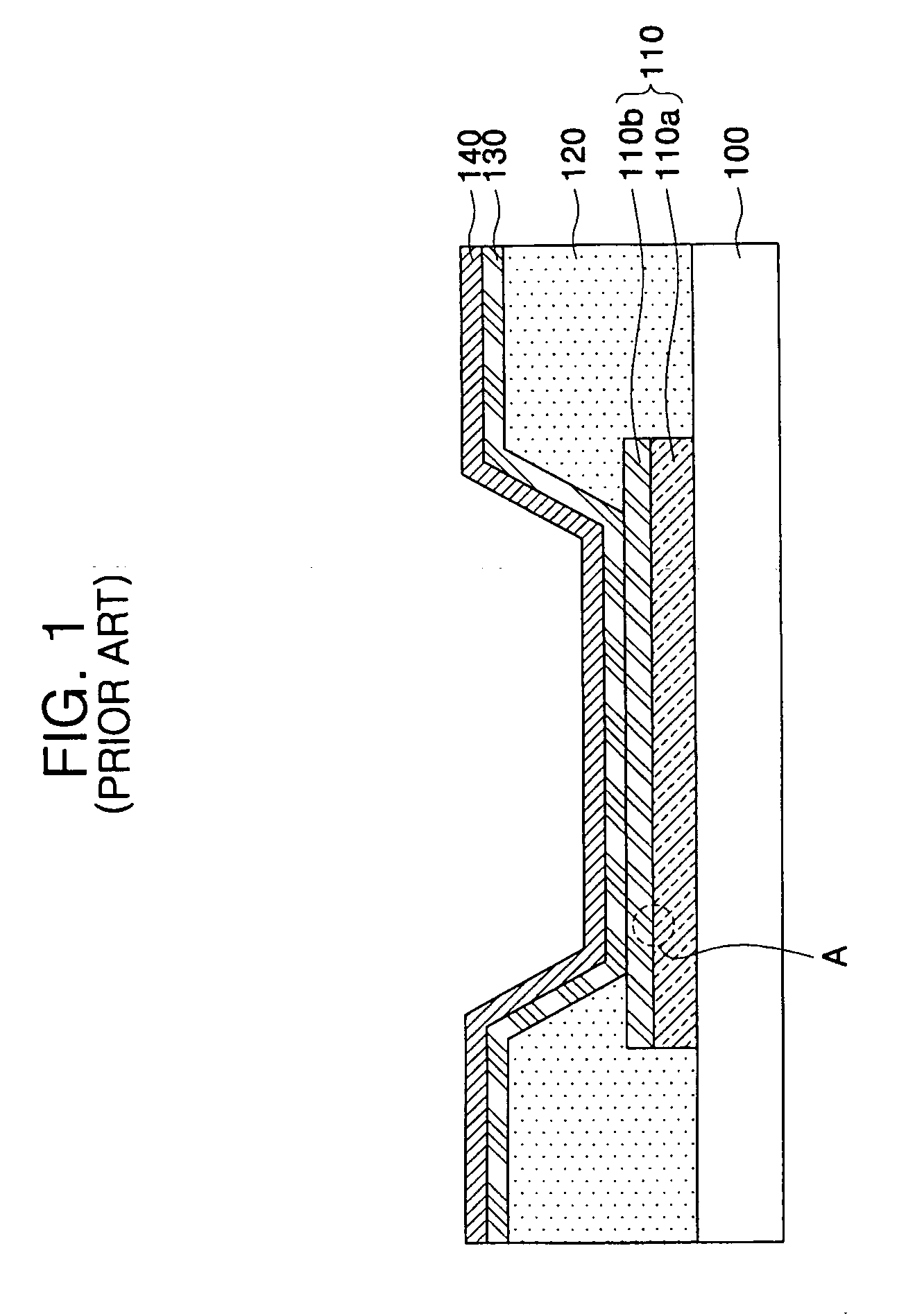
[0061]FIG. 4 is a graph illustrating a contact resistance measured at the Al—Si / ITO interface of the first electrode layer of the top-emission organic electroluminescent display obtained from the above example, and FIG. 5 is a graph illustrating a contact resistance measured at the AlNd / ITO interface of the top-emission organic electroluminescent display obtained from the above comparative example.
[0062] Referring to FIG. 4, resistance values measured in any regions of the first electrode layer are approximately equal, thereby showing that the contact resistance between the reflective layer and the transparent electrode layer is very stable. On the other hand, in FIG. 5, the measured resistance values are unevenly distribute...
PUM
 Abstract
Description
Claims
Application Information
 - R&D
- Intellectual Property
- Life Sciences
- Materials
- Tech Scout
- Unparalleled Data Quality
- Higher Quality Content
- 60% Fewer Hallucinations
Browse by: Latest US Patents, China's latest patents, Technical Efficacy Thesaurus, Application Domain, Technology Topic, Popular Technical Reports.
© 2025 PatSnap. All rights reserved.Legal|Privacy policy|Modern Slavery Act Transparency Statement|Sitemap|About US| Contact US: help@patsnap.com


