

Solder alloy, solder paste, solder ball, solder preform, solder joint, and substrate
- Summary
- Abstract
- Description
- Claims
- Application Information
AI Technical Summary
Benefits of technology
Problems solved by technology
Method used
Image

Examples
examples
[0104]1. Melting Point of Solder Alloy, 2. As Surface Concentration, 3. Suppression of Thickening Paste, 4. Suppression of Yellowing During Heating Solder Piece, 5. Tensile Strength, 6. Elongation, 6. Film Thickness of P-Rich Layer, 7. Shear Strength, and 8. Plate Exposure Rate were evaluated using solder alloys (mass %) shown in examples and comparative examples in Tables 1 to 8.
1. Melting Point of Solder Alloy
[0105]Melting points (° C.) of the solder alloys shown in Tables 1 to 8 were measured with a differential scanning calorimetry (DSC) (manufactured by Seiko Instruments Inc.: DSC6200) under the condition of a heating rate of 5° C. / min. In a case where the melting point was less than or equal to 185° C., it was evaluated as “O”. In a case where the melting point was greater than 185° C., it was evaluated as “X”.
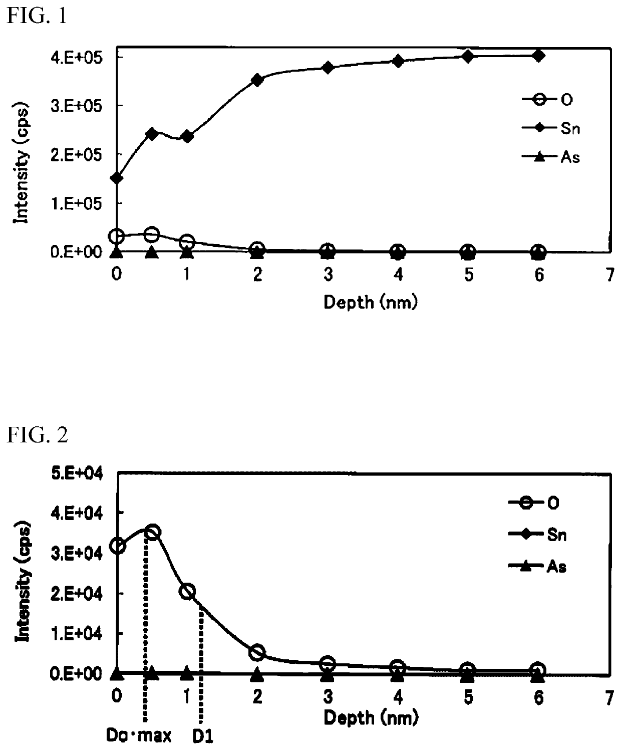
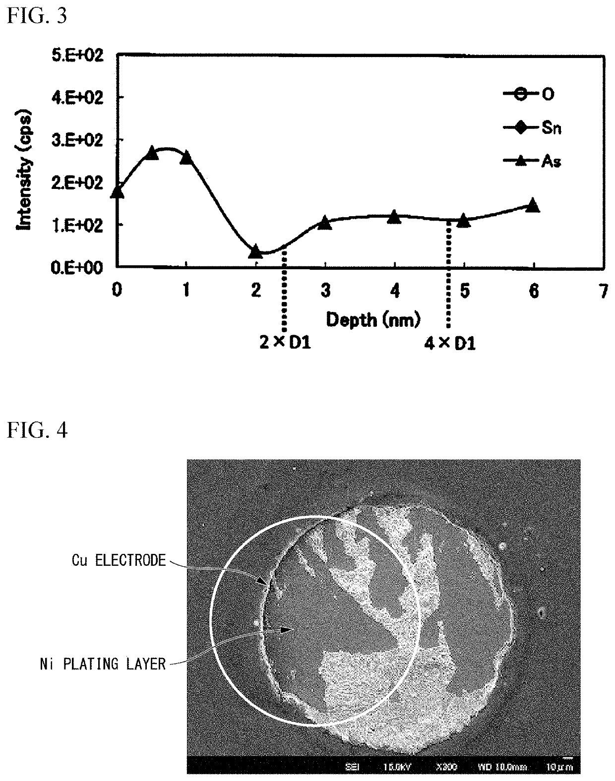
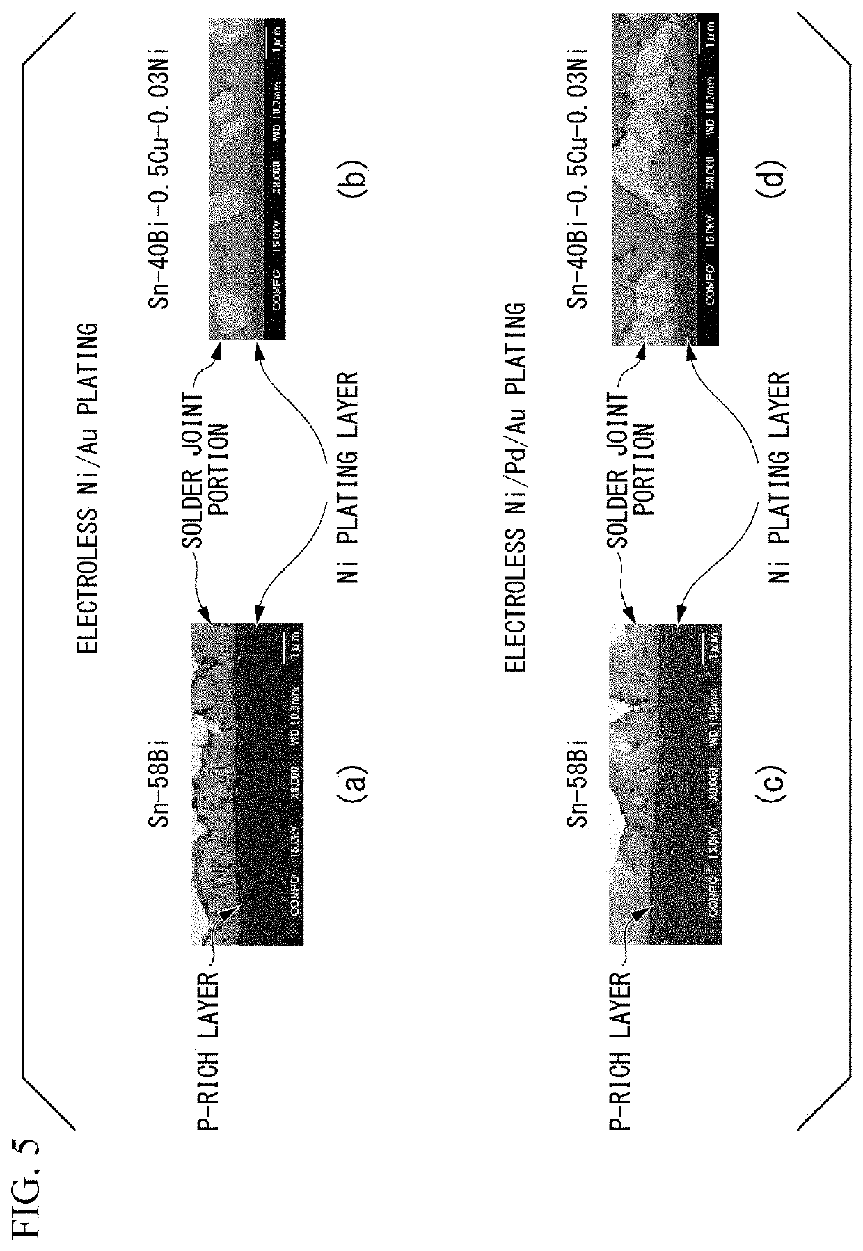
2. As Surface Concentration
[0106]The presence or absence of an As-concentrated layer was evaluated as follows using depth direction analysis through X-ray photoelectron ...
PUM
| Property | Measurement | Unit |
|---|---|---|
| Length | aaaaa | aaaaa |
| Length | aaaaa | aaaaa |
| Fraction | aaaaa | aaaaa |
Abstract
Description
Claims
Application Information