Nitride based semiconductor having improved external quantum efficiency and fabrication method thereof

a technology of external quantum efficiency and fabrication method, which is applied in the direction of semiconductor devices, storage devices, conveyors, etc., can solve the problems of poor etching process efficiency, v defects in p-cladding layers, and inability to form patterns smaller than micrometers, so as to improve external quantum efficiency and reduce internal reflection

Inactive Publication Date: 2005-10-13
SAMSUNG ELECTRO MECHANICS CO LTD
View PDF3 Cites 54 Cited by
  • Summary
  • Abstract
  • Description
  • Claims
  • Application Information

AI Technical Summary

Benefits of technology

[0011] The present invention has been made to solve the foregoing problems of the prior art and it is therefore an object of the present invention to provide a nitride semiconductor having a nanoscale roughened structure which is formed in an upper region of a p-capping layer via high temperature heat treatment to decrease internal reflection thereby improving external quantum efficiency.

Problems solved by technology

However, its etching process has poor efficiency because nitride semiconductors poorly react to acidic or basic etching solution.
However, there are drawbacks that the patterning process is to be added and it is impossible to form a pattern smaller than micrometer size.
However, the p-cladding layer may have for example V defects when grown in the low temperature range owing to defects such as dislocations (e.g., threading dislocations) which are connected from an n-cladding layer to an active layer.
This as a result heavily deteriorates reverse bias and electrostatic characteristics of a semiconductor device.

Method used


Image

  • Nitride based semiconductor having improved external quantum efficiency and fabrication method thereof
  • Nitride based semiconductor having improved external quantum efficiency and fabrication method thereof
  • Nitride based semiconductor having improved external quantum efficiency and fabrication method thereof

Examples


Embodiment Construction

[0037] The above and other objects, features and other advantages of the present invention will be more clearly understood from the following detailed description taken in conjunction with the accompanying drawings, in which:

[0038] Among terminologies used for explaining a nitride semiconductor and a fabrication method thereof of the invention, the terminology “low temperature range” designates a temperature range in which a p-capping layer of the nitride semiconductor maintains an amorphous or polycrystalline structure without crystallization, but the terminology “high temperature range” designates a temperature range in which the p-capping layer is at least partially phase transformed into a specific crystal structure.

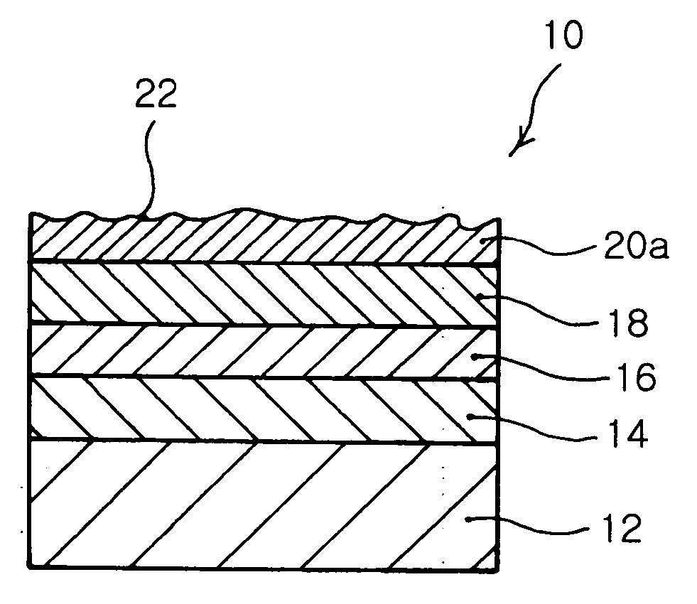
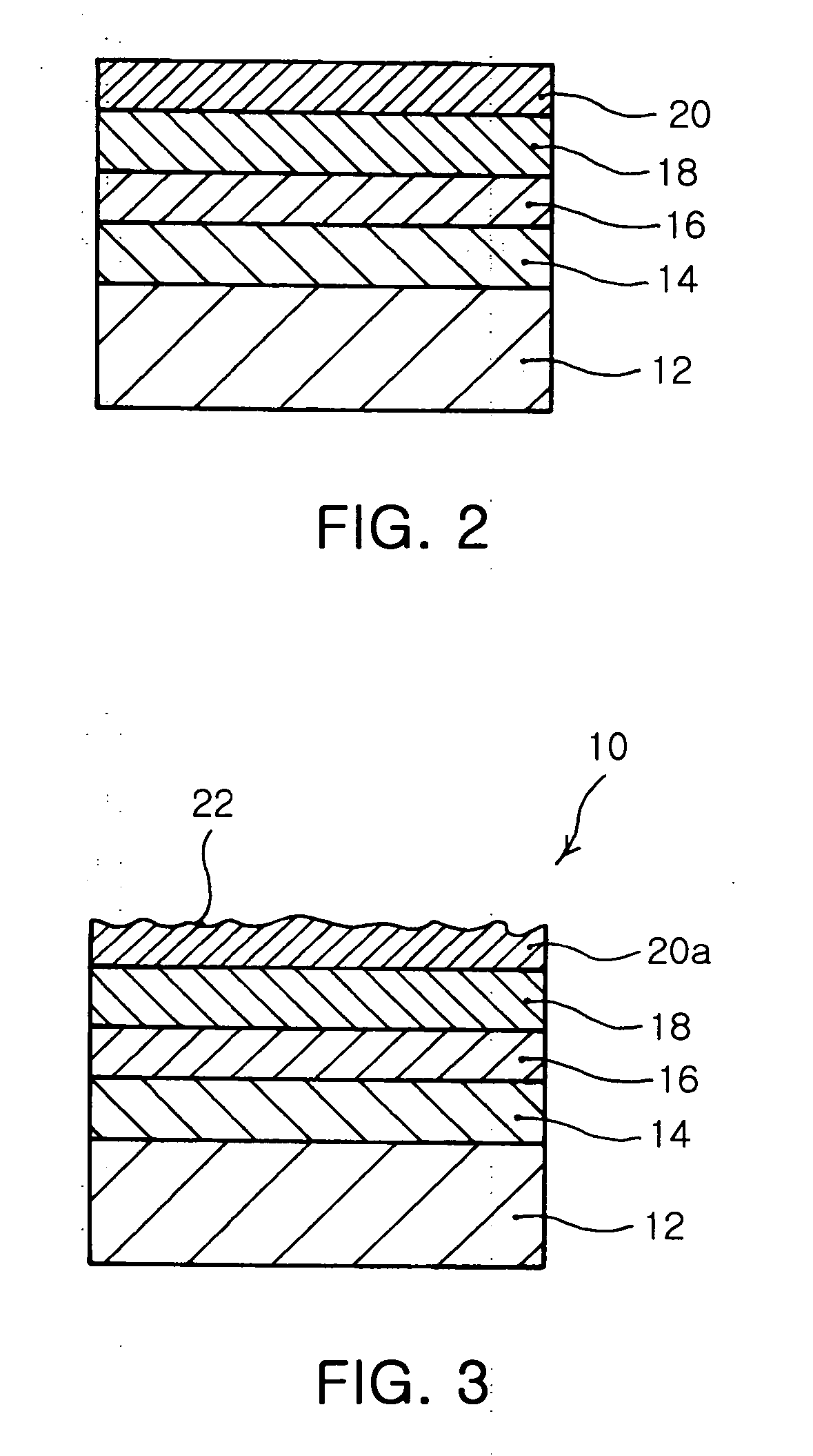
[0039] A structure of a nitride semiconductor 10 of the invention will be first described with reference to FIG. 3.

[0040] The nitride semiconductor 10 is used with an optoelectronic device such as an LED, and includes a transparent substrate 12 for example of sapp...


PUM

PropertyMeasurementUnit
temperatureaaaaaaaaaa
diameteraaaaaaaaaa

Abstract

A surface treated nitride semiconductor in use for a light emitting diode, in which an n-cladding layer is formed on a substrate. An active layer having a multiple quantum well structure is formed on the n-cladding layer. A p-cladding layer is formed on the active layer. A p-capping layer is formed on the p-cladding layer in a low temperature range in which single crystal growth does not take place. The p-capping layer has a nanoscale roughened structure formed in an upper surface thereof via heat treatment in a high temperature range in which at least partial crystallization takes place. The nanoscale roughened structure reduces total internal reflection of the nitride semiconductor thereby improving external quantum efficiency thereof.

Description

CLAIM OF PRIORITY [0001] This application claims the benefit of Korean Patent Application No. 2004-21802 filedonMar. 30, 2004, in the Korean Intellectual Property Office, the disclosure of which is incorporated herein by reference. BACKGROUND OF THE INVENTION [0002] 1. Field of the Invention [0003] The present invention relates to a nitride semiconductor in use for an optoelectronic device, and more particularly, to a nitride semiconductor having a nanoscale roughened structure in an upper region of a p-capping layer formed through high temperature heat treatment to reduce total internal reflection thereby improving external quantum efficiency and a fabrication method thereof. [0004] 2. Description of the Related Art [0005] In general, a nitride-based or nitride semiconductor for example of InAlGaN is used in a Light Emitting Doide (LED) for producing blue or green wavelength light. The nitride semiconductor has a representative formula of AlxInyGa(1-x-y)N, in which 0≦x≦1, 0≦y≦1 and...

Claims


Application Information

Patent Timeline
Patent Type & Authority Applications(United States)
IPC IPC(8): H01L27/15H01L33/22H01L33/32
CPCH01L33/22H01L33/32B65G1/026B65G2201/0267
Inventor KIM, SUN WOONOH, JEONG TAKLEE, KYU HANKIM, JE WON
Owner SAMSUNG ELECTRO MECHANICS CO LTD
Why Eureka
Try Eureka