Electro-optic modulators incorporating quantum dots

a quantum dots and optical modulator technology, applied in optics, instruments, nanotechnology, etc., can solve the problems of limited use in the telecom system, no universally accepted and adopted nomenclature for these types of materials, and the ferroelectric material lithium niobate is unsuitable for monolithic integration, etc., to improve the performance of electro-optic modulators, shorten the voltage, and improve the linear electro-optic effect

Inactive Publication Date: 2005-10-13
BOOKHAM TECH
View PDF8 Cites 13 Cited by
  • Summary
  • Abstract
  • Description
  • Claims
  • Application Information

AI Technical Summary

Benefits of technology

[0038] The invention, by using Quantum Dots (QDs) material to enhance the linear electro-optic effect permits improvements in the performance of electro-optic modulators, allowing them to be made shorter and/or lower voltage, and to operate over a broad range of wavelengths. Prior art proposals of modulators not using QDs, in particular in the InP systems which have different band-gap characteristics to G

Problems solved by technology

The concept of integrated optical (or ‘photonic’) circuits utilising a modulator to modulate a laser light beam is not new but, until recently, commercial—and hence telecom systems—use was limited to relatively simple devices, primarily lithium-niobate modulators, which are available from several commercial sources.
However, lithium niobate is a ferro-electric material unsuitable for monolithic integration such as desired for mass production of large scale integrated products to drive down unit cost.
However, there is as yet no universally accepted and adopted nomenclature for these types of materials, for example these types of materials are sometimes referred to as low dimension carrier confinement materials and other terms are also used.
The technology for producing QWs is well known but quantum wires have yet to be produced on a commercial scale.
In practise they have been formed in the laboratory by electrically constraining a QW structure with electrical fields, or by so called V-growth, but these are not yet a practical commercially available processes.
But an adverse feature of existing III-V semiconductor LEO effect modulators are their necessary length, typically 30 mm, due to the weak LEO effect, and the usual need to achieve a high depth of modulation.
In comparison with GaAs technolog

Method used


Image

  • Electro-optic modulators incorporating quantum dots
  • Electro-optic modulators incorporating quantum dots
  • Electro-optic modulators incorporating quantum dots

Examples


Embodiment Construction

[0055] The invention will now be described with reference to the accompanying drawings of which:

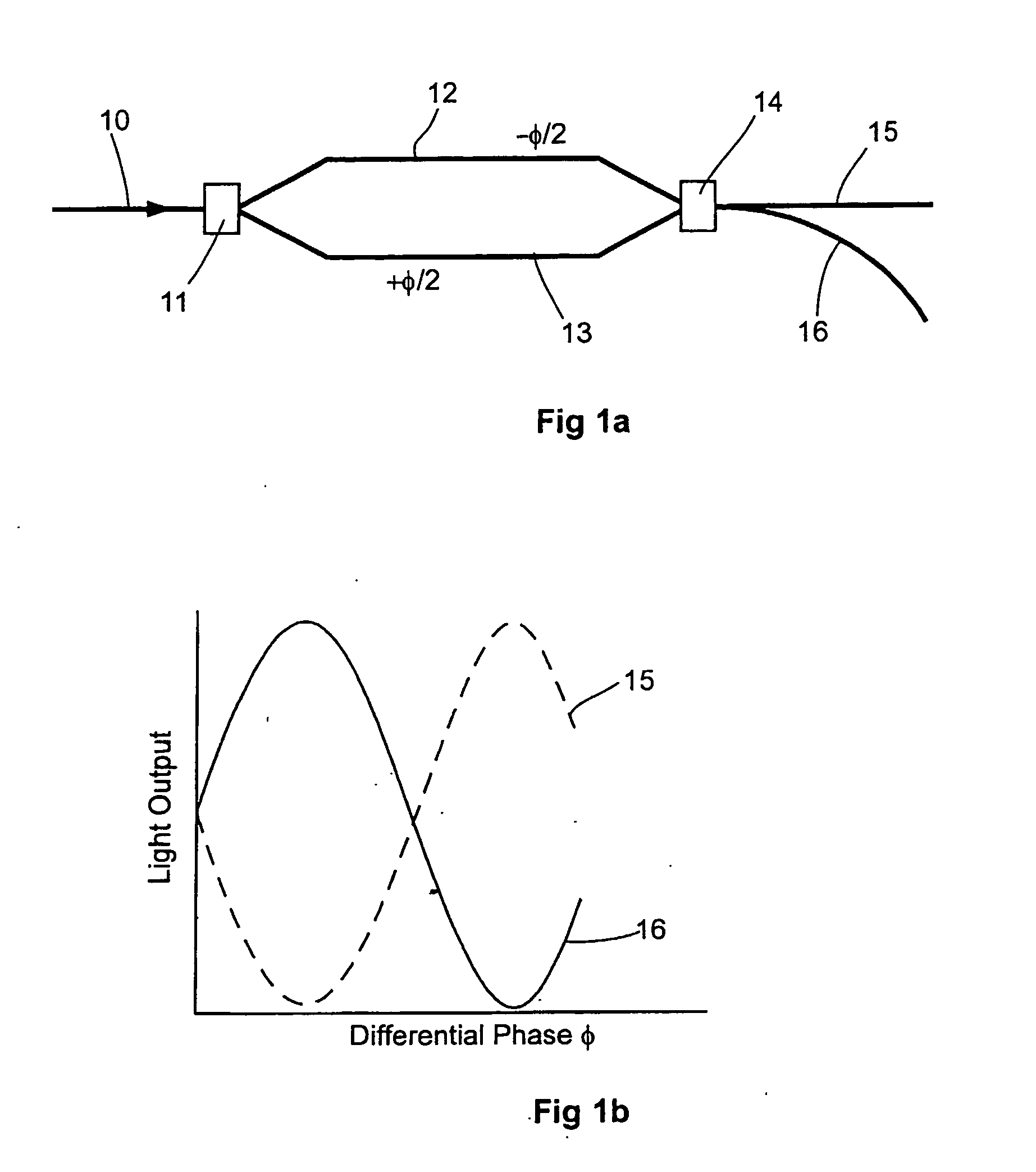
[0056]FIG. 1a. is a plan schematic view of a Mach Zehnder Interferometer (MZI),

[0057]FIG. 1b. is a graph of light output vs. differential phase,

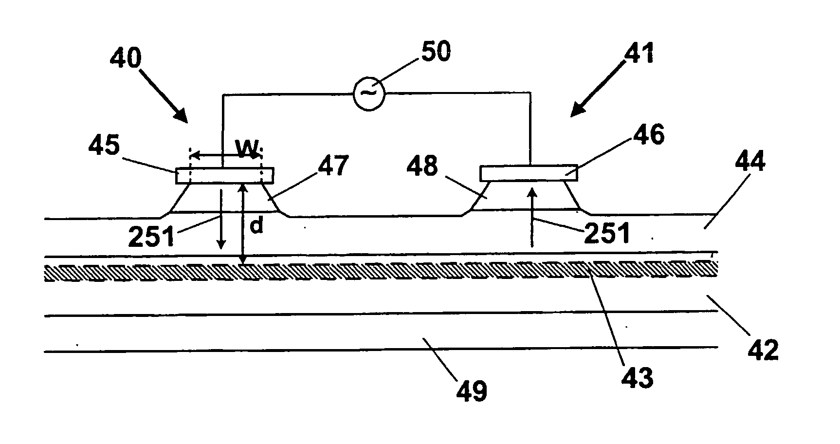
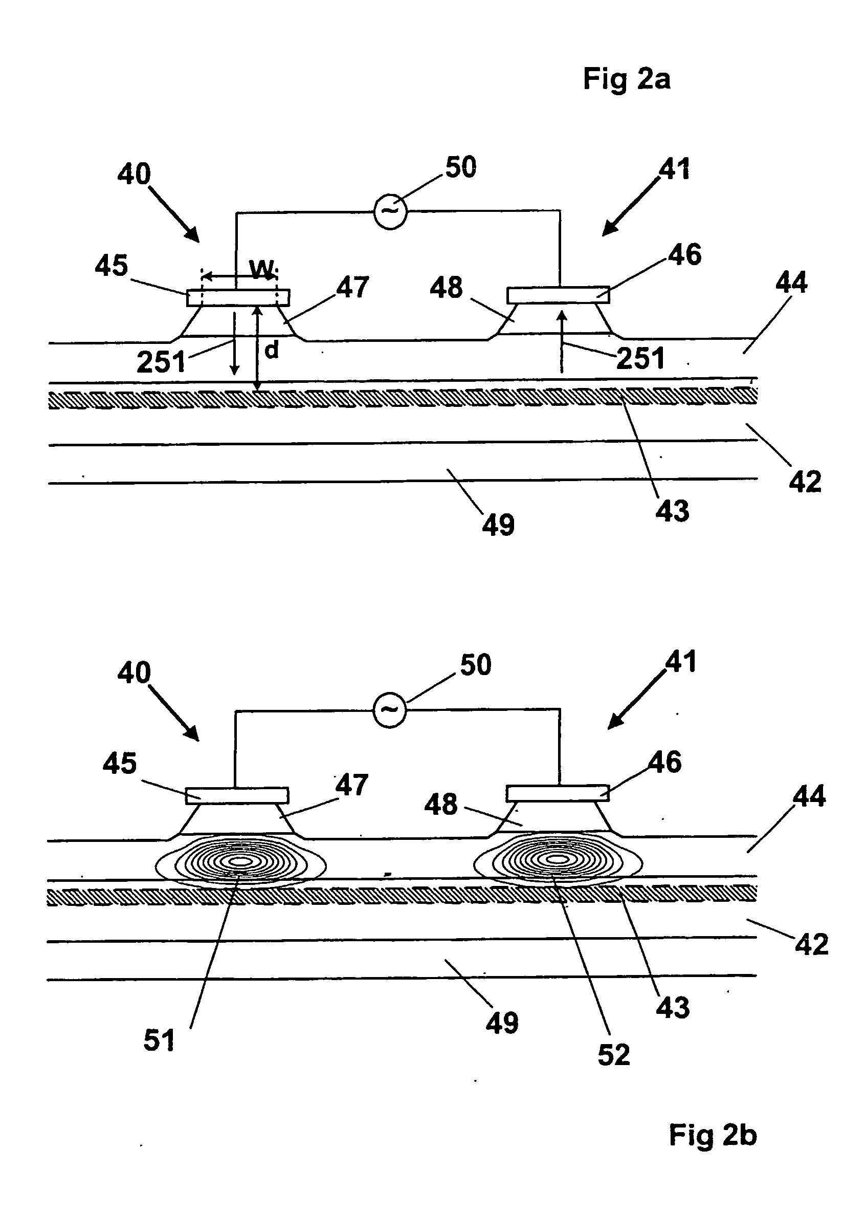
[0058]FIG. 2a. illustrates a cross section of a part of a series push-pull modulator based in semiconductor,

[0059]FIG. 2b. shows a cross section of a part of a series push-pull modulator based in semiconductor detailing the guided light profiles, and

[0060]FIG. 3. is a graph of the values r and s against wavelength λ.

DETAILED DESCRIPTION OF THE EMBODIMENTS

[0061] For ease of understanding, the invention will firstly be described with reference to an MZI format modulator, although it has wider uses than in MZIs alone and may be used in a variety of other known electro-optic modulator systems as described in Chapter 9, “Optical Electronics in Modern Communications”, A Yarif, Oxford University Press, ISBN 0-19-510626-1.

[0062] Referring to FIG. 1...


PUM


Abstract

A modulator is formed of a semiconductor material which utilises the electro-optic effect to achieve a change in the refractive index Δn of the material under the influence of an applied electrical field F (251), in accordance with the equation: Δn=−½ n03 [rF+sF2]≡ΔnL+ΔnQ where n0 is the refractive index of the material at zero field, and ΔnL and ΔnL and ΔnQ are the linear and quadratic contributions to the change in refractive index respectively, r is the linear electro-optic coefficient of the material and s is the quadratic electro-optic coefficient of the material incorporating a plurality of quantum dots and operating in a wavelength region where the value of rF is sufficiently greater than the value of sF2 so as to operate with the dominant effect on the refractive index Δn being contributed by the linear effect. In this way, a device with a wide bandwidth is achieved by appropriately separating the band-gap wavelength (λg) and the operating wavelengths (λ).

Description

[0001] This invention relates to electro-optic modulators and has particular reference to electro-optic modulators incorporating quantum dots for use, for example, in Mach-Zehnder interferometers (MZIs). BACKGROUND [0002] In this specification the term “light” will be used in the sense that it is used in optical systems to mean not just visible light but also electromagnetic radiation having a wavelength between 800 nanometres (nm) and 3000 nm. [0003] The present invention is concerned with a modulator for modulating an extant laser beam. The concept of integrated optical (or ‘photonic’) circuits utilising a modulator to modulate a laser light beam is not new but, until recently, commercial—and hence telecom systems—use was limited to relatively simple devices, primarily lithium-niobate modulators, which are available from several commercial sources. However, lithium niobate is a ferro-electric material unsuitable for monolithic integration such as desired for mass production of lar...

Claims


Application Information

Patent Timeline
IPC IPC(8): G02F1/017G02F1/225
CPCB82Y20/00G02F1/01708G02F2203/04G02F2001/01791G02F1/2257G02F1/01791
Inventor ZAKHLENIUK, NICKHOLDEN, ANTHONY JAMES
Owner BOOKHAM TECH
Why Eureka
Try Eureka