Solid-state laser pumped by semiconductor laser array

a laser array and solid-state technology, applied in the field of laser technology, can solve the problems of limited heat dissipation efficiency, increased laser number, and increased optical source size, and achieve the effect of improving laser oscillation efficiency and low cos

Inactive Publication Date: 2005-10-13
RICOH KK
View PDF16 Cites 14 Cited by
  • Summary
  • Abstract
  • Description
  • Claims
  • Application Information

AI Technical Summary

Benefits of technology

[0030] Accordingly, it is a general object of the present invention to provide a novel and useful solid-state laser apparatus wherein the foregoing problems are eliminated.
[0031] Another and more specific object of the present invention is to provide a high-power solid-state laser apparatus pumped by a semiconductor laser and capable of providing plural laser beams of different wavelengths in a visible wavelength band, such that there is caused efficient laser oscillation and such that the solid-state laser apparatus can be formed with low cost in the form of compact package.
[0032] Another object of the present invention is to provide a compact and high-power solid-state laser apparatus of the type noted above such that the laser apparatus has a microchip construction characterized by a compact cavity size and realizes highly efficient laser excitation by causing the optical pumping by using a semiconductor laser array as a pumping optical source, the optical pumping of the solid-state laser being achieved in the direction perpendicular to the direction in which the output laser beam is produced for improving the heat resistance of the material constituting the solid-state laser, the laser apparatus having the construction suitable for assembling and mounting with low cost by using an automated facility by arranging and mounting the solid-state laser and the semiconductor laser array on a common mounting substrate. It should be noted that the present invention seeks for the construction capable of forming the solid-state laser apparatus in the form of a compact package by using the foregoing construction.

Problems solved by technology

On the other hand, the optical source of this prior art, relying on the mechanism of heat dissipation conducted from an edge of a sapphire substrate for cooling the laser crystal, has a drawback of limited efficiency of heat dissipation, and it is difficult to obtain large laser output.
However, such increase of the number of the lasers inevitably increases the size of the optical source.
On the other hand, this prior art has a drawback, associated with its use of laser output mirror, in that the size of the optical source cannot be reduced.
Further, because it is necessary with this prior art laser optical source to irradiate a pumping optical beam selectively to the region where the rare earth element has been added, and associated with this, various complex problems are caused in relation to the optical system used for the pumping optical beam or in relation to the shape of the laser crystal.
Thus, it is difficult with this prior art to reduce the cost of the optical source.
However, this conventional art also uses laser mirrors, and it is not possible to reduce the size of the optical source.
Further, because this prior art causes the pumping of the disk-shaped laser crystal for the entirety thereof, it is not possible to increase the efficiency of wavelength conversion.
In addition, this prior art has a drawback, in relation to its construction of pumping the disk-shaped laser crystal as a whole, in that overlapping of the laser oscillation region and the pumping region in the laser crystal (mode matching efficiency) cannot be increased when the pumping is made from the lateral direction.
While this drawback may be resolved by providing a core part doped with the rare earths at the central part of the disk-shaped laser crystal, it is still difficult to reduce the size of the optical source as a whole in view of the pumping action made from the entire azimuth directions of the laser crystal and further in view of the construction in which the laser crystal and the pumping source are disposed with separation Heretofore, the conventional solid-state laser optical sources of single wavelength have been reviewed.
Thus, the output power of the laser array is rather limited.
Further, the variable range of the wavelength is limited by the bandgap.
This means that the wavelength range of this optical source is limited and the use thereof for the application of projectors is not appropriate.
However, this prior art suffers from the problems in that, while it is certainly possible to form three-primary color laser beams with this prior art, the output power thereof is limited because of the use of semiconductor lasers, and it becomes necessary to mount a large number of semiconductor lasers for obtaining large output power.
However, the use of semiconductor lasers with large number increases the complexity of construction of the optical source and raises a further problem of handling a large number of laser beams.
Thereby, designing of the optical system becomes inevitably complex.
Thus, there exists no known high-luminosity laser optical source of compact size and still capable of providing high output power.
Further, there is no known construction of compact and high-power laser optical source that can reduce the cost thereof.
Further, there exists no known construction for providing the laser beams of plural wavelengths simultaneously such that the laser beams of different wavelengths are formed with reduced spatial separation in the same unit.

Method used


Image

  • Solid-state laser pumped by semiconductor laser array
  • Solid-state laser pumped by semiconductor laser array
  • Solid-state laser pumped by semiconductor laser array

Examples


example 1

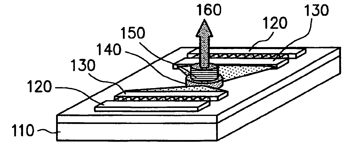
[0083] First, Example 1 will be explained with reference to FIGS. 1A and 1B, wherein FIG. 1A is a diagram showing the construction of the solid-state laser of the present example, while FIG. 1B shows the solid-state laser medium used in the solid-state laser of FIG. 1A in a front view and a side view.

[0084] Referring to FIG. 1A, the solid-laser apparatus of Example 1 is constructed on a mounting substrate 110 and includes, on the mounting substrate 110, semiconductor laser arrays 120 for pumping, microlens elements 130 cooperating with the respective semiconductor laser arrays 120, a solid-state laser medium 140 and a wavelength conversion element 150.

[0085] In the present example, the mounting substrate 110 comprises a flat substrate of aluminum nitride having a size of 50×50 mm and a thickness of 5 mm.

[0086] Thereby, it will be noted that there are disposed two semiconductor laser array elements 120, each producing an optical output of 20 W at the wavelength of 808 nm, on the m...

example 2

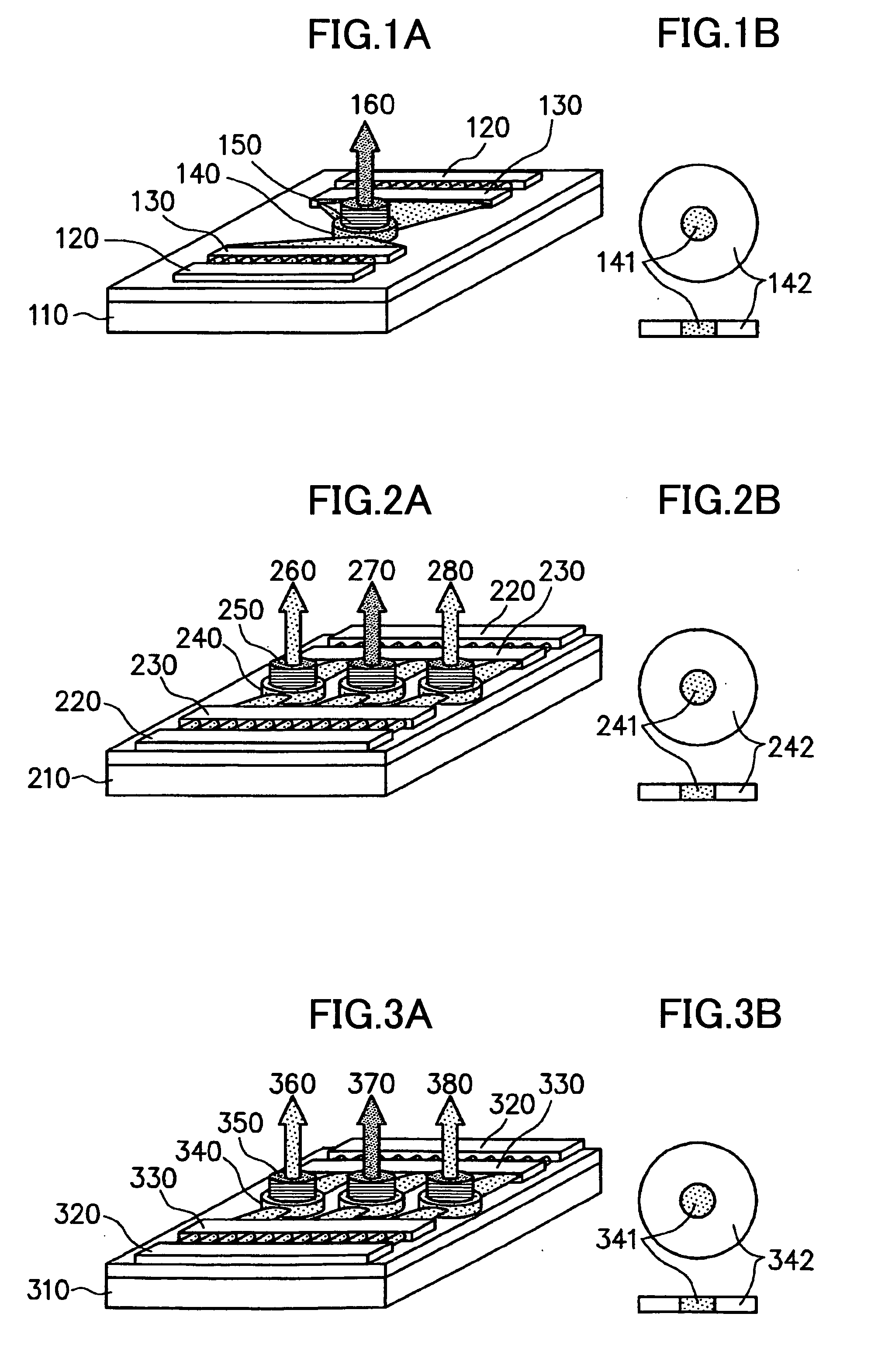
[0109] Next, Example 2 of the present invention will be described with reference to FIGS. 2A and 2B, wherein FIG. 2A shows the construction of the solid-state laser apparatus of the present embodiment, while FIG. 2B shows the laser medium used with the laser apparatus of FIG. 2A in a front view and a side view.

[0110] Referring to Embodiment 2, the laser apparatus is constructed on a mounting substrate 210 and includes a semiconductor laser array 220, microlenses 230, a laser medium 240 and a wavelength conversion element 250, wherein the laser arrays 220, the microlenses 230 and the laser medium 240 are all mounted directly on the mounting substrate 210. The wavelength conversion element 250 is provided on the laser medium 240.

[0111] Here, it should be noted that the mounting substrate 210 comprises a flat board of an aluminum nitride having a size of 50×50 mm and a thickness of 5 mm.

[0112] On the other hand, the semiconductor laser array 220 produces a pumping laser beam with th...

example 3

[0151] Next, Example 3 will be explained with reference to FIGS. 3A and 3B, wherein FIG. 3A is a diagram showing the construction of the solid-state laser of the present example, while FIG. 3B shows the solid-state laser medium used in the solid-state laser of FIG. 3A in a front view and a side view.

[0152] Referring to FIG. 3A, the solid-laser apparatus of Example 3 is constructed on a mounting substrate 310 and includes, on the mounting substrate 310, semiconductor laser arrays 320 for pumping, microlens elements 330 cooperating with the respective semiconductor laser arrays 320, a solid-state laser medium 340 and a wavelength conversion element 350.

[0153] In the present example, the mounting substrate 310 comprises a flat substrate of aluminum nitride having a size of 50×50 mm and a thickness of 5 mm.

[0154] Thereby, it will be noted that there are disposed two semiconductor laser array elements 320, each producing an optical output of 30 W at the wavelength of 808 nm, on the mo...


PUM


Abstract

A solid-state laser apparatus includes a solid-state laser medium producing an output laser beam, the solid-state laser medium forming a microchip laser and having opposing end surfaces forming a laser cavity, a semiconductor laser array pumping the solid-state laser medium by a pumping laser beam, the semiconductor laser array injecting the pumping laser beam to the solid-state laser medium from a direction perpendicular to a direction of the output laser beam, the solid-state laser medium and the semiconductor laser array are mounted on a common mounting substrate.

Description

BACKGROUND OF THE INVENTION [0001] The present invention relates in general to laser technology and more particularly to a solid-state laser pumped by a semiconductor laser. More specifically, the present invention relates to a solid-state laser pumped by semiconductor lasers and equipped with a wavelength-conversion element. Such a semiconductor laser can oscillate at plural, different wavelengths and is applicable to laser printers, laser scanning display devices, laser projectors, and the like. [0002] Recently, various apparatuses that use laser beam are put into practical use. Such apparatuses include optical disk apparatuses, laser printers, laser instruments, and the like. Further, investigations are being made for laser display devices in the prospect of future practical use. [0003] In these applications, there exist various demands such as shortening of the laser oscillation wavelength, providing of three primary colors (red, blue, green), and the like. Thus, development of ...

Claims


Application Information

Patent Timeline
Patent Type & Authority Applications(United States)
IPC IPC(8): H01S3/00H01S3/042H01S3/06H01S3/091H01S3/0941H01S3/109H01S3/16H01S3/23
CPCH01S3/005H01S3/025H01S3/042H01S3/0604H01S3/0612H01S3/0627H01S3/2391H01S3/109H01S3/1611H01S3/1643H01S3/1671H01S3/2383H01S3/0941
Inventor SUZUDO, TSUYOSHITAIRA, TAKUNORI
Owner RICOH KK
Why Eureka
Try Eureka