Method and apparatus for producing a 3-D model of a semiconductor chip from mosaic images

Inactive Publication Date: 2005-10-13
CHIPWORKS INC
View PDF5 Cites 6 Cited by
  • Summary
  • Abstract
  • Description
  • Claims
  • Application Information

AI Technical Summary

Benefits of technology

[0018] It is therefore an object of the invention to provide a method and apparatus that achieves improved alignment between mosaic images of respective

Problems solved by technology

Operator intervention is only required to verify putative line segments th

Method used


Image

  • Method and apparatus for producing a 3-D model of a semiconductor chip from mosaic images
  • Method and apparatus for producing a 3-D model of a semiconductor chip from mosaic images
  • Method and apparatus for producing a 3-D model of a semiconductor chip from mosaic images

Examples


Example

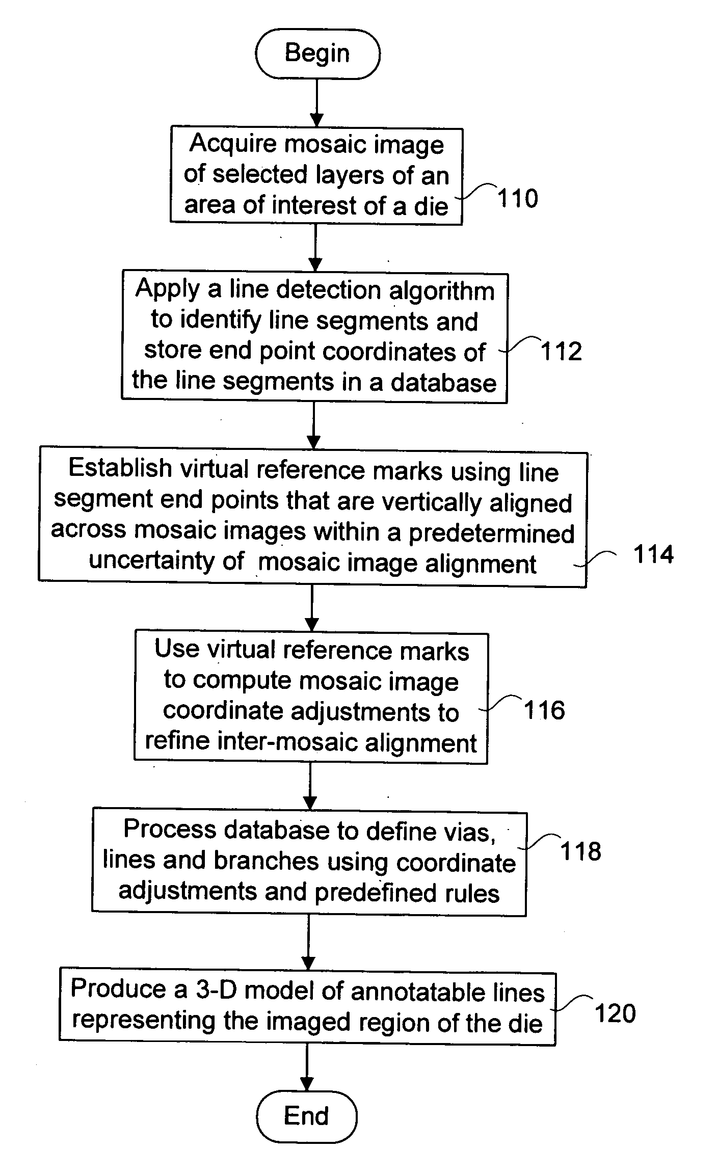
[0038] The invention provides a method for producing a 3-D model of the connectivity of a semiconductor chip from a plurality of image mosaics corresponding to respective layers of an area of interest on the semiconductor chip.

[0039]FIG. 4 schematically illustrates an image processing workstation 50 in accordance with an embodiment of the invention. Workstation 50 includes a processor 52 for executing program instructions stored in a memory 54. The memory 54 stores program instructions for carrying out the automated processes of line detection 56, mosaic image alignment 58, and 3-D model generation 60, each of which is further discussed below.

[0040] The workstation 50 is adapted to receive the coarsely aligned mosaic image data from the mosaic image database 48, and to apply a line detection algorithm effected using the line detection 56 program instructions. The data output of the line detection algorithm is stored in a corresponding line segment database 62. A plurality of line ...


PUM


Abstract

A three-dimensional model of a semiconductor chip is produced from coarsely aligned mosaic images of respective layers of the semiconductor chip using an improved method for aligning the mosaic images, so that minimal operator intervention is required to produce the model. A line detection algorithm is applied to each of the mosaic images to produce a set of line segments identified by x and y coordinates of end points of the line segments with respect to a frame defined by a mosaic image in which each line segment occurs. Virtual reference marks are established using end points of different mosaic images that are vertically aligned to within an uncertainty of the coarse alignment of the mosaic images, and the virtual reference marks are used to compute a mean adjustment of the x and y coordinates of each of the mosaic images to produce a three dimensional coordinate space. The end points are processed within the three dimensional coordinate space to define vias, lines and branch lines of the semiconductor chip, which are used to build the three-dimensional model. Operator intervention is only required to verify putative line segments that are marked as uncertain because of poor agreement with predefined rules. The 3-D model may be annotated and viewed separately from the mosaic images.

Description

CROSS-REFERENCE TO RELATED APPLICATIONS [0001] This is the first application filed for the present invention. MICROFICHE APPENDIX [0002] Not Applicable. TECHNICAL FIELD [0003] The invention generally relates to the analysis of integrated circuits, and in particular, to a method and system for producing a 3-D model of metal lines in layers of a semiconductor chip. BACKGROUND OF THE INVENTION [0004] The reverse engineering of semiconductor chips is an important enterprise in today's technology market, and can be used for product verification, market intelligence purposes, and identifying infringement of intellectual property rights. Semiconductor chips generally include a polysilicon layer and a plurality of metal layers. It is well known to produce mosaic images of an area of interest on a semiconductor chip by stitching together highly magnified images of small parts of the area of interest on each layer of the chip. The images are acquired using an iterated process that alternates ...

Claims


Application Information

Patent Timeline
IPC IPC(8): G06F7/60G06F17/50G06F19/00G06K9/36G06T5/00G06T5/50G06T7/00
CPCG06K9/00134G06K2009/2045G06T7/0028G06T2207/30148G06T17/10G06T2200/08G06T2207/10056G06T7/0083G06T7/33G06T7/12G06V20/693G06V10/16
Inventor LACHANCE, ALEXANDER R.BLAXELL, ZYGO
Owner CHIPWORKS INC
Why Eureka
Try Eureka