Semiconductor device

a technology of semiconductor devices and metal thin films, applied in the direction of solid-state devices, semiconductor/solid-state device details, metal rolling arrangements, etc., can solve the problems of deformation of the reliability of the semiconductor device, deformation of the insulating film or silicon substrate, and induced electron-hole pairs in the silicon substrate, etc., to reduce the resistance value of the metal thin-film resistance on the underlying film, stabilize the resistance value of the metal thin-film resistance, and suppress the variation of the resistance value of the metal

Inactive Publication Date: 2005-10-20
RICOH KK
View PDF3 Cites 5 Cited by
  • Summary
  • Abstract
  • Description
  • Claims
  • Application Information

AI Technical Summary

Benefits of technology

[0047] Thus, the present invention provides a semiconductor device capable of eliminating irradiation of laser beam upon the semiconductor substrate at the time of laser trimming process in which a laser beam having an intensity sufficient to cause disconnection or modification in the metal thin-film resistance is irradiated.
[0117] Also, in the semiconductor device including an output driver controlling an output of an input voltage, a voltage divider for producing a divided voltage by dividing the output voltage, a reference voltage generator for producing a reference voltage, and a comparator circuit comparing the divided voltage from the voltage divider and the reference voltage from the reference voltage generator and controlling the operation of the output driver in response to the result of comparison, it becomes possible to improve the precision of the output voltage of the voltage divider by using the metal thin-film resistance of the present invention for the resistance elements of the voltage divider and by using the laser beam interruption film. Thus, the output voltage of the constant voltage generator is stabilized.

Problems solved by technology

With the conventional semiconductor device explained with reference to FIGS. 35 through 40, there has been a problem in that, upon irradiation of the semiconductor substrate such as a silicon substrate via an insulation film such as a silicon oxide film with the laser beam at the time of trimming of the metal thin-film resistance, the irradiated laser beam causes damages in the insulation film or silicon substrate and the reliability of the semiconductor device is degraded.
Further, there has been a problem at the time of on-line trimming process in that electron-hole pairs are induced in the silicon substrate as a result of irradiation of the laser beam upon the silicon substrate.
Such electron-hole pairs cause noise at the time of performance measurement, and it has been difficult to carry out precise trimming.
In order to avoid such problems, it is necessary to set the laser power to the range between a minimum power capable of disconnecting or modifying the metal thin-film resistance and the maximum power in which the semiconductor substrate undergoes modification, while it should be noted that such a range is narrow and stable trimming is difficult.

Method used


Image

  • Semiconductor device
  • Semiconductor device
  • Semiconductor device

Examples


Embodiment Construction

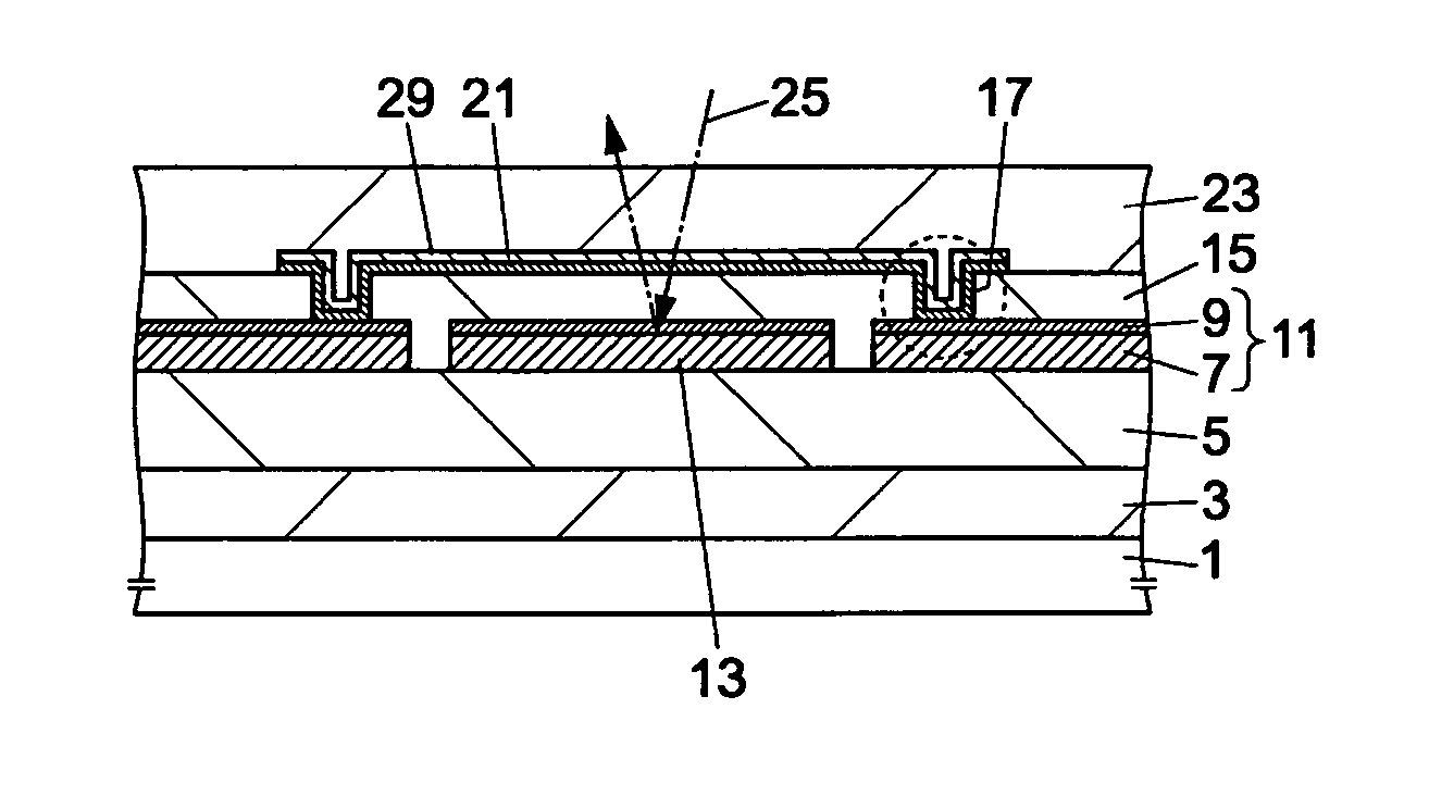
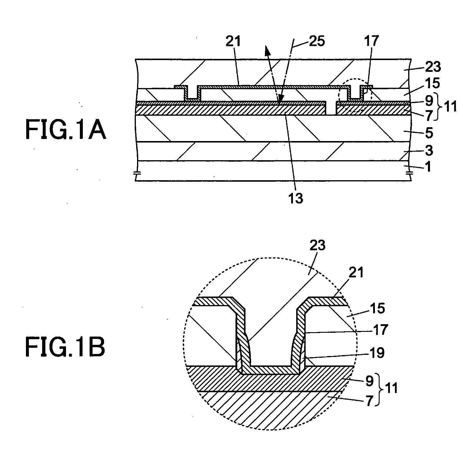
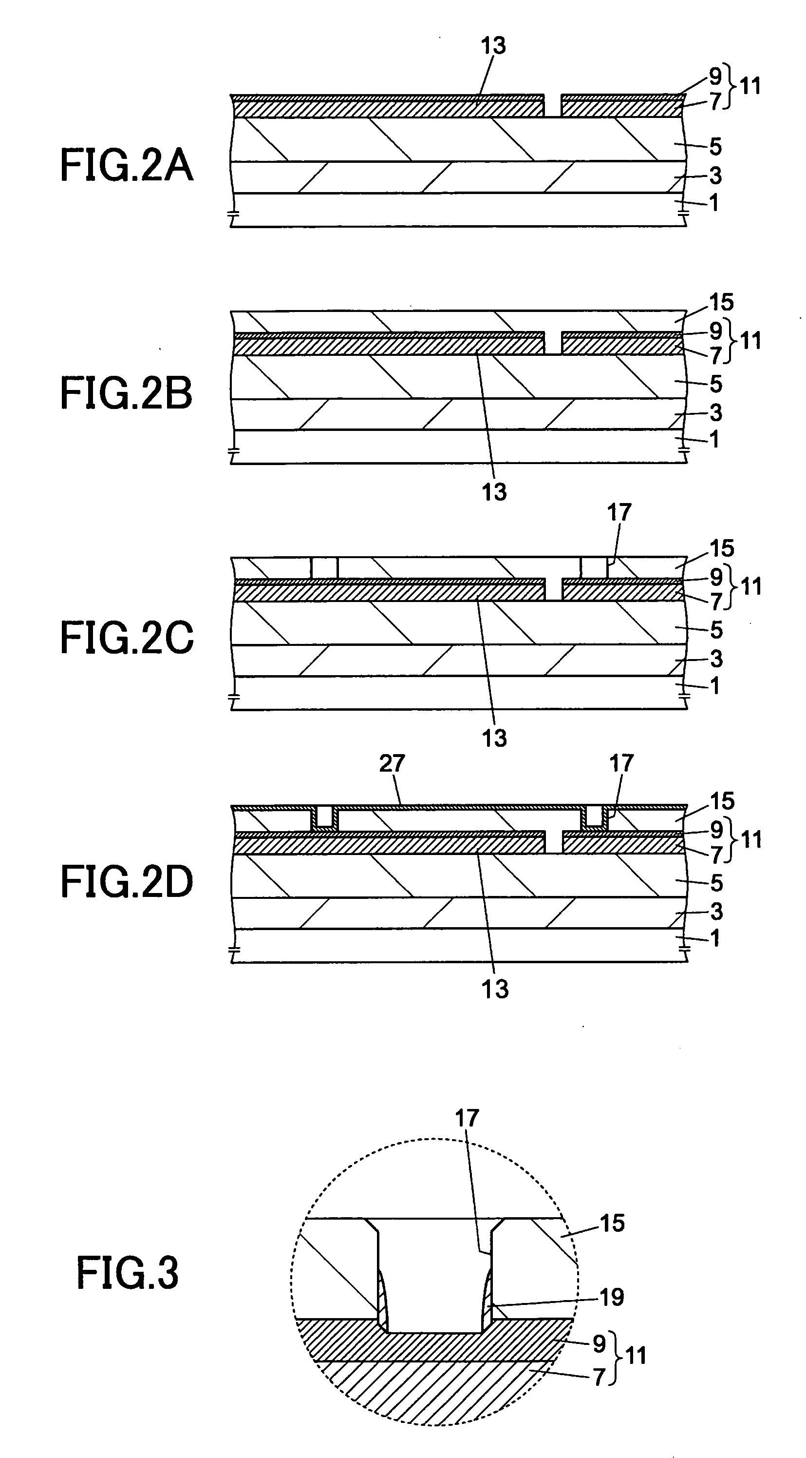
[0158]FIGS. 1A and 1B are cross-sectional diagrams showing an embodiment of the first mode of the present invention wherein FIG. 1A is a cross-sectional view showing a region where a metal thin-film resistance is formed while FIG. 1B is an enlarged cross-sectional diagram showing a part of FIG. 1A circled by a broken line. In the embodiments described hereinafter, it should be noted that transistors or capacitors are formed on the same substrate while illustration thereof are omitted.

[0159] On a silicon substrate 1, there is formed a device isolation oxide 3, and a first layer interlayer insulation film (lower insulation film) is of BPSG (borophosphosilicate grass) or a PSG (phosphosilicate glass) is formed on the silicon substrate 1 including the region where the device isolation oxide 3 is formed. Further, a first layer metal interconnection pattern 11 of a metal pattern 7 and a refractory metal film 9 formed on the metal pattern 7 is formed on the first layer interlayer insulati...


PUM

PropertyMeasurementUnit
thicknessaaaaaaaaaa
thicknessaaaaaaaaaa
thicknessaaaaaaaaaa

Abstract

A semiconductor device includes a base insulation film formed on a semiconductor substrate via another layer, a metal thin-film resistance formed on the base insulation film, and a laser beam interruption film of a metal material interposed between the semiconductor substrate and the base insulation film.

Description

BACKGROUND OF THE INVENTION [0001] The Present invention generally relates to semiconductor devices and more particularly to a semiconductor device having a metal film resistance formed of a metal thin-film, which in turn is formed on an insulation film. [0002] Resistance elements constitute an important part of analog integrated circuit. [0003] Particularly, a resistance element of a metal thin-film (called hereinafter as metal thin-film resistance) attracts attention in view of its small temperature dependence of the resistance value (TCR). [0004] For the material of such metal thin-film resistance, chromium-silicon (CrSi), nickel chromium (NiCr), tantalum nitride (TaN), chromium silicide (CrSi2), chromium silicide nitride (CrSiN), chromium silicon oxy (CrSiO), and the like, are used. [0005] With a semiconductor device having such a metal thin-film resistance, it is generally practiced to form the metal thin-film resistance with very small thickness of 1000 Angstroms or less in or...

Claims


Application Information

Patent Timeline
Patent Type & Authority Applications(United States)
IPC IPC(8): H01L27/04B21B1/00B21C1/00B21F1/00H01C7/00H01L21/822H01L27/01
CPCH01L27/016H01C7/006
Inventor KATO, HIDENORIMORI, MASAHIDE
Owner RICOH KK
Why Eureka
Try Eureka