Semiconductor device and method for manufacturing the same

a technology of semiconductor devices and semiconductors, applied in the direction of electromagnets with armatures, non-metallic protective coating applications, electrical apparatus construction details, etc., can solve the problems of limited operating temperature of control elements, increased size, and lower operating temperature, and achieves the effect of not increasing the manufacturing cost of devices, small size, and easy mounting in actuators

Inactive Publication Date: 2005-10-20
DENSO CORP
View PDF22 Cites 64 Cited by
  • Summary
  • Abstract
  • Description
  • Claims
  • Application Information

AI Technical Summary

Benefits of technology

[0072] An electric device includes: a heat sink; an electric device disposed on the heat sink; a lead frame disposed around the electric device; and a resin mold molding the heat sink, the electric device, and the lead frame in such a manner that a bottom of the heat sink is exposed from the resin mold. The lead frame includes a suspending lead connecting to the heat sink. The resin mold includes an upper portion and a lower portion. The upper portion of the resin mold is disposed above the suspending lead. The lower portion of the resin mold is disposed below the suspending lead, and the lower portion is protruded from the upper portion. In this case, a dead space around the upper surface of the heat sink is reduced appropriately. Thus, the device has a small size so that the device is mounted in an actuator with ease.
[0073] Further, a method for manufacturing an electric device includes the steps of: mounting an electric element on an upper surface of a heat sink; mounting a lead frame around the electric element; connecting the heat sink to a suspending lead of the lead frame; and molding the heat sink, the electric element, and the lead frame with a resin mold by using a mold in such a manner that a bottom of the heat sink is exposed from the resin mold. The step of molding with the resin mold includes the steps of: pressing the suspending lead with a top mold of the mold; pressing the bottom of the heat sink on a bottom mold of the mold; and pouring melted resin into a cavity of the mold. The above method provides the electric device having no dead space on the upper surface of the heat sink, i.e., the mounting surface of the heat sink, on which the electric element is mounted. Further, no additional equipment such as a suction device is necessitated for the above method, so that the manufacturing cost of the device is not increased.

Problems solved by technology

The control element is limited in operating temperature and usually has a lower operating temperature because it has delicate construction as compared with the power element.
In simple terms, it is recommendable to increase the distance between the control element and the power element on the wiring board on which the control element and the power element are mounted, but in this case, the device results in increasing in size, which is not desirable.
That is, in the semiconductor device like this, it can be an important problem to prevent heat transfer from the second electronic element to the first electronic element.
However, in the conventional electronic device described above, large heat is transmitted to a temperature-limited element from a heating element that is larger in the amount of current and in the amount heat generation than the temperature-limited element via a heat sink easily transmitting heat, whereby the temperature-limited element is susceptible to the heat.
The temperature-limited element is limited in operating temperature and usually has a low operating temperature because it has finer construction than the heating element such as power element.
However, this results in increasing the size of the device, which is not preferable.
However, under these circumstances, when an electronic device is mounted in an actuator to make an integrated assembly, there is a tendency that the enlarged size of electronic device, as described above, increases space for mounting the electronic device in the actuator and makes it difficult to secure the space for mounting the electronic device.
When the electronic device is required to have multiple pins, and when Al thick wires are used as bonding wires, the spaces between the connection terminals need to be elongated or the bonding parts of the connection terminals need to be enlarged in size, which leads to the increased size of the device and by extension to increased cost.
Further, in the case of element that is small in size and needs many wire connections, it is difficult to make the wire connections by use of the Al thick wires.
However, Au thin wire can not respond to large current.
Further, Au thin wire also presents a problem that, usually, Au thin wire can not be bonded to connection terminal nonelectrolytically plated with Ni.
However, as described above, when the surface of connection terminal is not nonelectrolytically plated with Ni, weldability can not be secured in the connection between the connection terminal and the external part.
Further, the bonding of Al wire to the connection terminal electroplated with Ni is difficult in securing flatness as compared with the bonding of Al wire to the connection terminal nonelectrolytically plated with Ni and hence can not be performed with ease.
This prevents high package density and increases the size and cost of the device.
However, in this case, there is a possibility that the bonding portion is displaced by the pressing force to displace the lead frame with respect to the heat sink.
However, according to the method described above, a mold does not press the surface of a heat sink on which electronic elements are mounted and hence dead space is not provided.
However, the method requires a manufacturing machine provided with a suction unit and hence raises a problem of upsizing of the machine and increasing cost.

Method used


Image

  • Semiconductor device and method for manufacturing the same
  • Semiconductor device and method for manufacturing the same
  • Semiconductor device and method for manufacturing the same

Examples


first embodiment

[0114] A first embodiment of the present invention relates to a semiconductor device provided with a first electronic element such as control element and a second electronic element such as power element that has larger current passed therethrough as compared with the first electronic element to generate large heat and is used for driving an actuator, for example, a motor.

[0115] The inventors have investigated that a problem to be described in the following arose in the case of a semiconductor device according to a related art.

[0116]FIG. 5 is a circuit block diagram to show the typical circuit construction of a semiconductor device as a HIC for driving the driving motor of power window of an automobile. Specifically, FIG. 5 is the circuit block diagram to show a common circuit construction of the semiconductor device as a HIC for driving a driving motor of a power window of an automobile and having a JAM function.

[0117] In FIG. 5, a control element 10 as the first electronic elem...

second embodiment

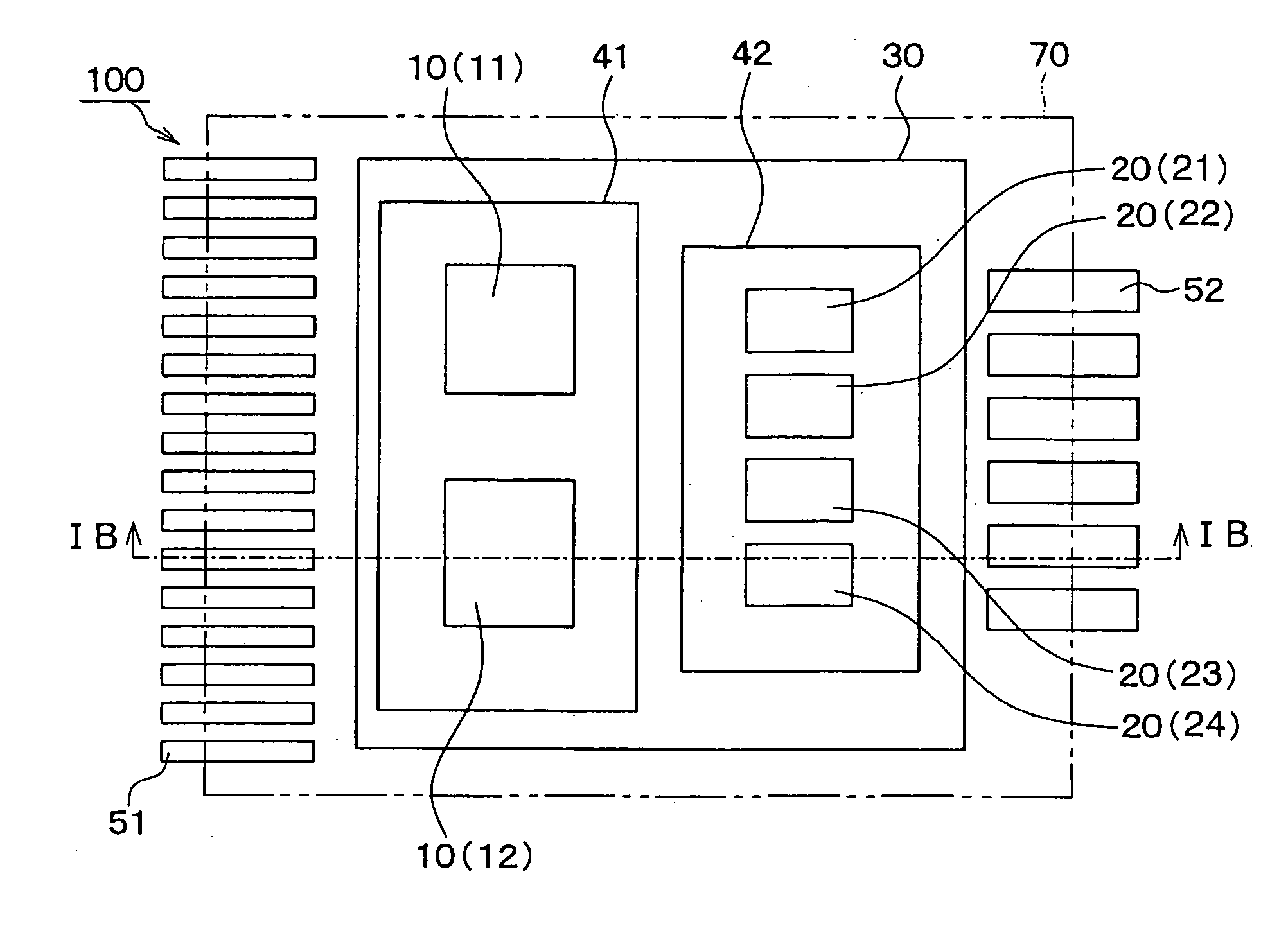
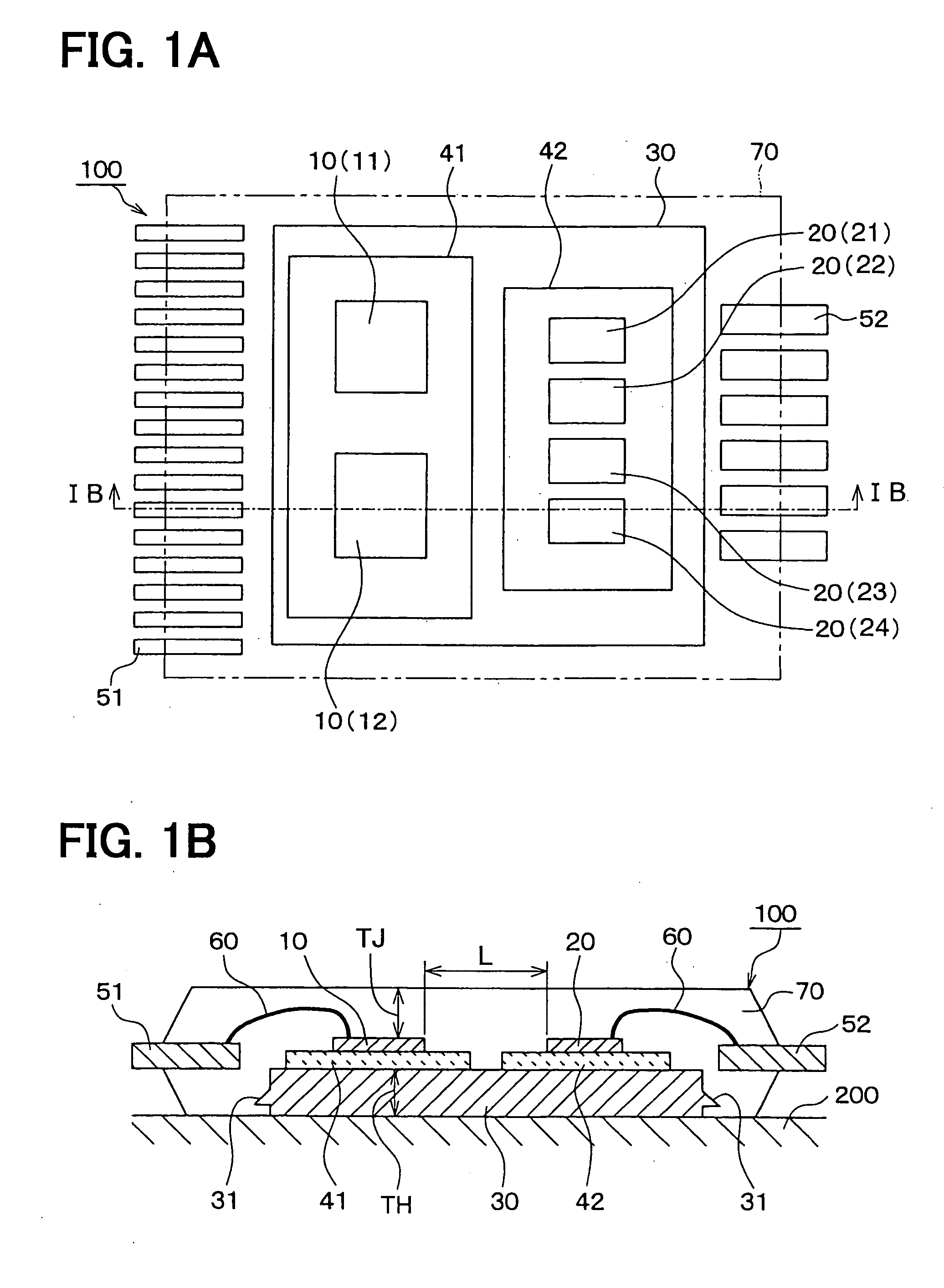
[0276]FIGS. 12A and 12B are illustrations to show the schematic construction of the semiconductor device 200 provided with the first electronic element 10 and the second electronic element 20 in accordance with a second embodiment of the present invention and FIG. 12A is a plan view and FIG. 12B is a sectional view along a line XIIB-XIIB in FIG. 12A.

[0277] Further, FIG. 13A is a schematic sectional views of a temperature sensing diode 90 formed in the control IC 12 in the semiconductor device 200 shown in FIGS. 12A and 12B, and FIG. 13B is a schematic sectional view of a temperature sensing diode 90 formed in the power MOS elements 21, 24 in the semiconductor device 200 shown in FIGS. 12A and 12B.

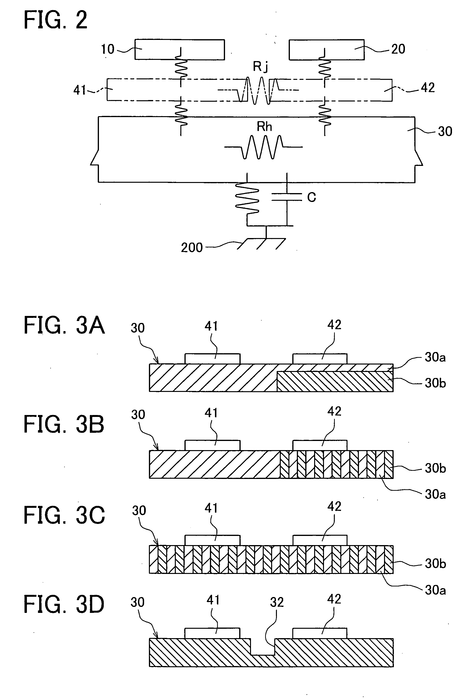
[0278] Also in this embodiment, there is provided a semiconductor device provided with the control element 10 and the power element 20 controlled by the control element 10 and characterized in that: the device is provided with the heat sink 30, the first wiring board 41 and the second wir...

third embodiment

[0339] A third embodiment of the present invention relates to an electronic device made by mounting a heating element and a temperature-limited element on a heat sink and then by molding them in such a manner as to wrap them by a molding resin.

[0340]FIG. 19 is an illustration to show a schematic plan construction of an electronic device 300 provided with a heating element 20 as the second electronic element and a temperature-limited element 10 as the first electronic element in accordance with a third embodiment of the present invention.

[0341] Further, FIG. 20 is an illustration to show a schematic sectional construction of the electronic device 300 shown in FIG. 19. Here, in FIG. 19, bonding wires 60 are omitted and in FIG. 20, some of bonding wires are omitted.

[0342] In this embodiment, descriptions will be provided on the assumption that the electronic device 300 is applied to a HIC (hybrid IC, hybrid integrated circuit) for driving the driving motor of power window of an auto...


PUM

PropertyMeasurementUnit
thicknessaaaaaaaaaa
diameteraaaaaaaaaa
diameteraaaaaaaaaa

Abstract

An electric device includes: a first electric element; a second electric element capable of flowing large current therethrough so that heat is generated in the second electric element; a heat sink; and a first wiring board and a second wiring board, which are disposed on one side of the heat sink. The large current in the second electric element is larger than that in the first electric element. The first wiring board and the second wiring board are separated each other. The first electric element is disposed on the first wiring board, and the second electric element is disposed on the second wiring board.

Description

CROSS REFERENCE TO RELATED APPLICATIONS [0001] This application is based on Japanese Patent Applications No. 2004-118889 filed on Apr. 14, 2004, No. 2004-171220 filed on Jun. 9, 2004, No. 2004-171221 filed on Jun. 9, 2004, No.2004-175419 filed on Jun. 14, 2004, No. 2004-175420 filed on Jun. 14, 2004, No. 2004-200448 filed on Jul. 7, 2004, and No. 2004-291398 filed on Oct. 4, 2004, the disclosures of which are incorporated herein by reference. FIELD OF THE INVENTION [0002] The present invention relates to a semiconductor device and a method for manufacturing the semiconductor device. BACKGROUND OF THE INVENTION [0003] Among conventional semiconductor devices provided with the first electronic element and the second electronic element that has larger current passed therethrough as compared with the first electronic element to generate large heat is, for example, a semiconductor device having a control element such as microcomputer as the first electronic element and having a power ele...

Claims


Application Information

Patent Timeline
Patent Type & Authority Applications(United States)
IPC IPC(8): H01F7/18H01L21/56H01L23/36H01L23/433H01L23/488H01L23/495H01L25/04H05K1/02H05K1/03H05K1/14H05K3/28H05K7/02
CPCH01L21/565H01L2924/1305H01L23/4952H01L23/49562H01L23/49575H01L24/45H01L24/49H01L2224/45015H01L2224/45124H01L2224/45144H01L2224/48091H01L2224/48247H01L2224/48472H01L2224/4903H01L2224/49051H01L2224/49171H01L2224/49175H01L2224/73265H01L2924/01005H01L2924/01006H01L2924/01013H01L2924/01014H01L2924/01015H01L2924/01028H01L2924/01029H01L2924/01046H01L2924/01047H01L2924/01074H01L2924/01078H01L2924/01079H01L2924/01082H01L2924/01083H01L2924/09701H01L2924/13055H01L2924/13091H01L2924/14H01L2924/19041H01L2924/19042H01L2924/19043H01L2924/19105H01L2924/19107H01L2924/20752H01L2924/20753H01L2924/2076H01L2924/3011H05K1/0263H05K1/0306H05K1/142H05K3/0061H05K3/284H05K2201/10924H05K2203/049H01L24/48H01L2924/01019H01L2924/01023H01L2924/01033H01L2924/01045H01L2924/01068H01L2924/014H01L2224/32225H01L2224/48227H01L2224/48095H01L2224/49111H01L23/4334H01L2924/00014H01L2924/00H01L2924/00012H01L2924/351H01L2924/181H01L24/73
Inventor FUKUDA, YUTAKASAITOU, MITSUHIRONAGAYA, TOSHIHIROKINOUCHI, KANAKAMA, SADAHIRONUMAZAKI, KOJIIMAIZUMI, NORIHISAHAYASHI, HIROMASAFUKATSU, AKIHIROKASUYA, HIROKAZUUEDA, NOBUMASA
Owner DENSO CORP
Why Eureka
Try Eureka