Method for forming self-aligned contact in semiconductor device

a self-aligning contact and semiconductor technology, applied in semiconductor/solid-state device manufacturing, basic electric elements, electric devices, etc., can solve the problems of reducing the efficiency of semiconductor devices, so as to improve the problem of junction leakage, short-circuit and short-circuiting between bitlines can be effectively prevented

Active Publication Date: 2005-10-27
NAN YA TECH
View PDF6 Cites 170 Cited by
  • Summary
  • Abstract
  • Description
  • Claims
  • Application Information

AI Technical Summary

Benefits of technology

[0014] It is an object of the invention is to provide a method for forming a self-aligned contact in a semiconductor device, which is adapted for use in fabrication of memory arrays to eliminate the possibility of over-etching of a nitride cap layer and spacers to thereby prevent short-circuiting between a wordline and a bitline.
[0015] Another object of the invention is to provide a method for forming a self-aligned contact in a semiconductor device, which is adapted for use in fabrication of memory arrays to reduce the junction loss caused during the formation of a contact hole to thereby improve the junction leakage.
[0016] A further object of the invention is to provide a method for forming a self-aligned contact in a semiconductor device, which is adapted for use in fabrication of memory arrays to eliminate the possibility of joining of adjacent contacts even if voids are produced in the inter-layer dielectric (ILD) during the process to thereby prevent short-circuiting between bitlines.
[0020] As described above, in the present invention, the contact hole is formed by removing the plug portion of doped oxide with the vapor hydrofluoric acid. Therefore, undesired over-etching at a corner portion of the nitride insulating layer for protecting the gate structure can be avoided, and thus short-circuiting between the wordline and the bitline can be effectively prevented. Moreover, since the vapor hydrofluoric acid does not erode the nitride insulating layer, it is possible to ensure a junction loss of less than 50 Å, which effectively improves the problem of junction leakage. In addition, when the nitride insulating layer is formed on side walls of the plug portion, undesired joining of adjacent contacts can be avoided and thus short-circuiting between bitlines can be effectively prevented.

Problems solved by technology

However, in a semiconductor process having a feature size of 70 nm or less, the following problems will occur when adopting the conventional SAC technique.
Therefore, it is difficult to prevent over-etching of the nitride.
This causes exposure of the gate to the contact, leading to short-circuiting between the wordline and the bitline.
Second, the etchant used in the formation of the contact hole also erodes the junction region in the substrate.
When the feature size is reduced, junction depth becomes shallow; for example, for the 70 nm process, the junction depth is only about 200 Å. Therefore, loss of the silicon substrate results in a considerable junction leakage.

Method used


Image

  • Method for forming self-aligned contact in semiconductor device
  • Method for forming self-aligned contact in semiconductor device
  • Method for forming self-aligned contact in semiconductor device

Examples


Embodiment Construction

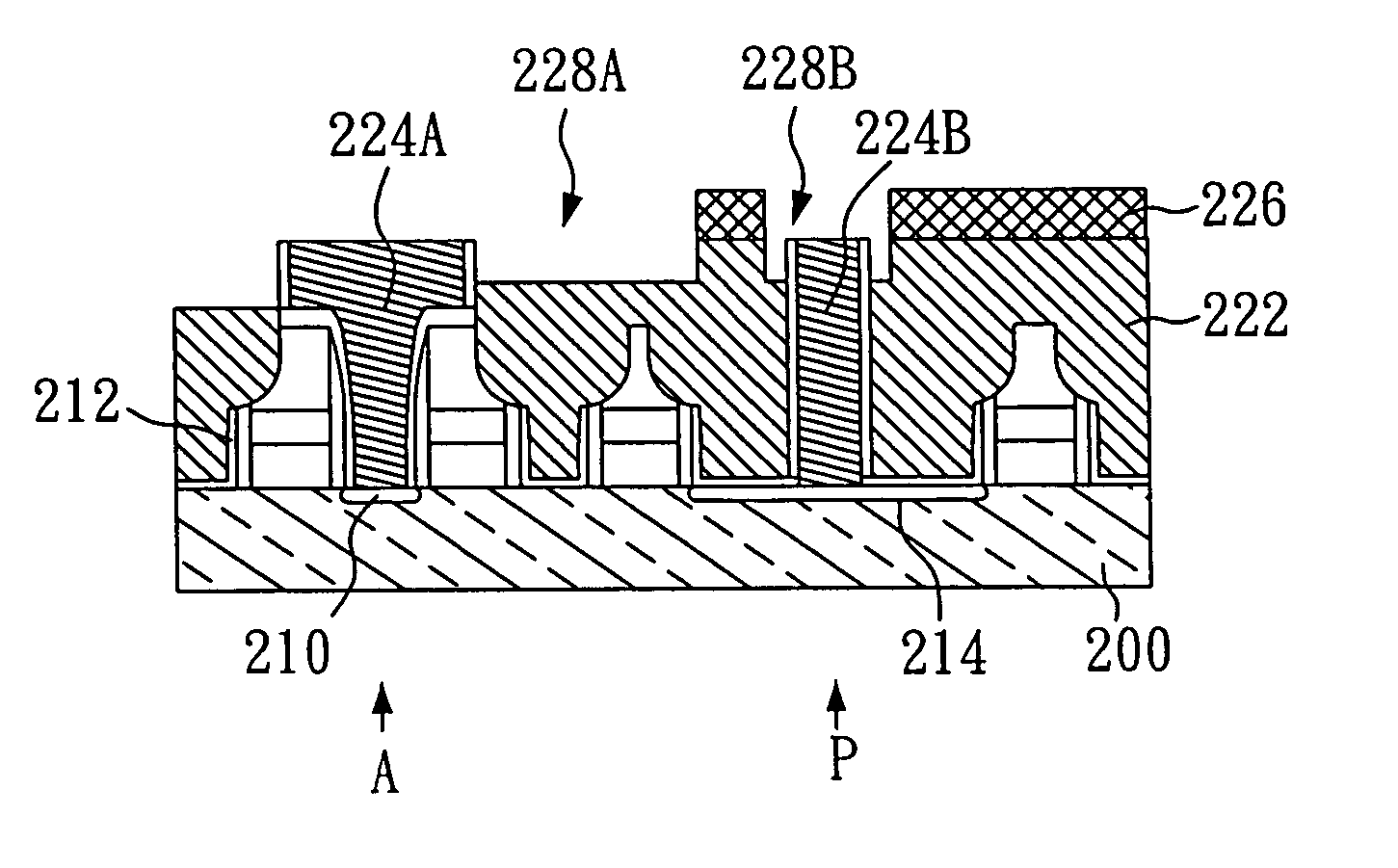
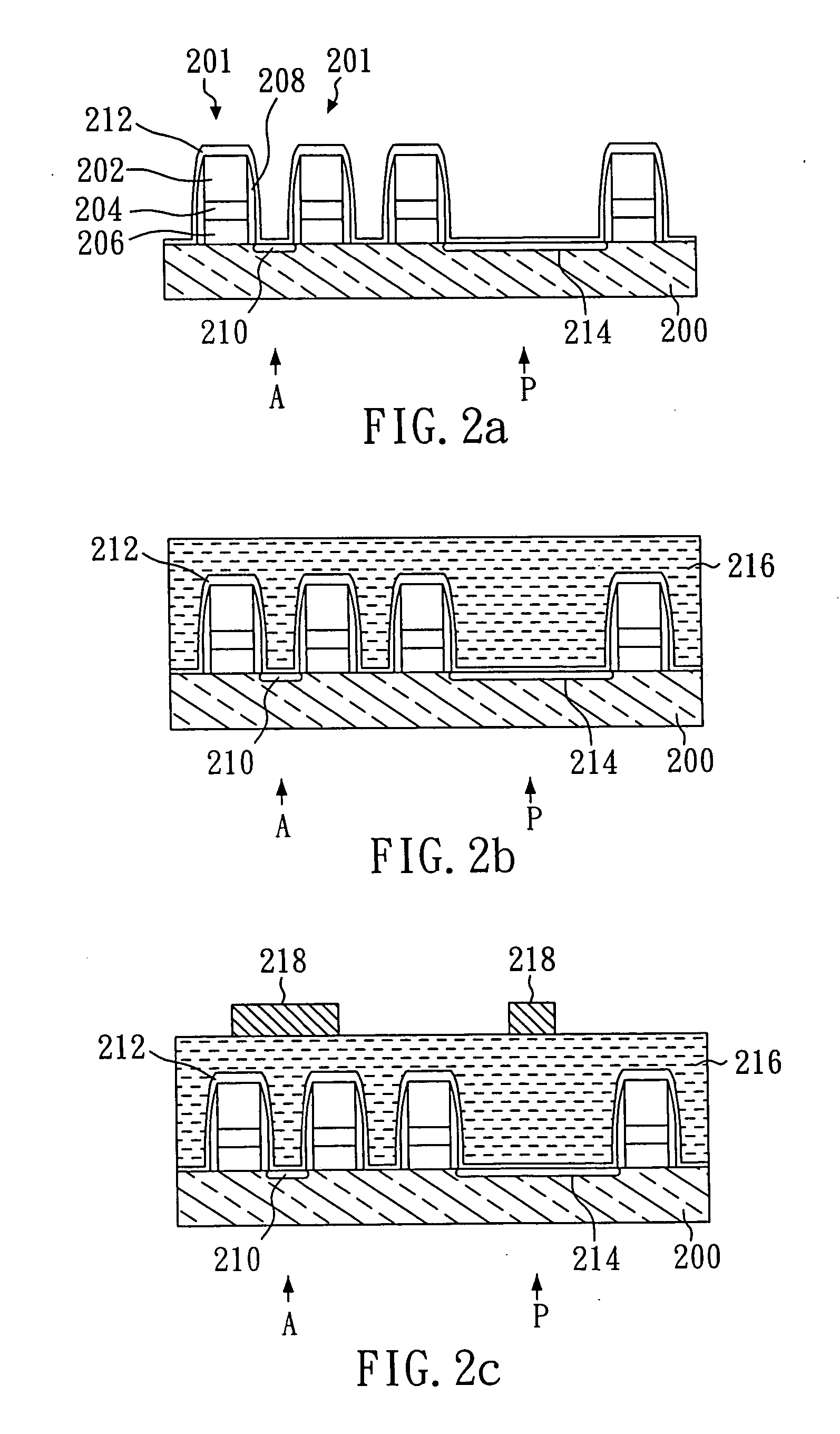
[0024] The method of forming a self-aligned contact in a semiconductor device according to the present invention will be explained with reference to the cross-sectional views in FIGS. 2(a) to 2(h).

[0025] According to a preferred example of the present invention, bitline contacts in a memory array area of a memory device and other contacts required in a periphery area can be formed in the same process.

[0026] In FIG. 2(a), the memory array area is on the left side, designated by an arrow A, while the periphery area is on the right side, designated by an arrow P.

[0027] According to the preferred example of the present invention, first, a plurality of gate structures 201 are provided on a substrate 200, and junction regions 210 and 214 are formed in the substrate 200 by ion implantation. Similar to the prior art in FIG. 1, the gate structure 201 includes a polysilicon (poly-Si) layer 206 and a tungsten silicide (WSix) layer 204 on the polysilicon layer 206. The tungsten silicide laye...


PUM

PropertyMeasurementUnit
feature sizeaaaaaaaaaa
junction depthaaaaaaaaaa
insulatingaaaaaaaaaa

Abstract

A method for forming a self-aligned contact on a semiconductor substrate provided with a plurality of field-effect transistors. The method comprises the steps of forming a first insulating layer comprising a nitride along a profile of a gate structure and a junction region, forming a temporary layer comprising a doped oxide on the first insulating layer, removing a portion of the temporary layer by performing a selective etch of the oxide with a mask while leaving a plug portion of the temporary layer over the junction region, forming a second insulating layer comprising an undoped oxide in a region where the portion of the temporary layer is removed, removing the plug portion by performing a selective etch of the undoped oxide to form a contact hole, removing a portion of the first insulating layer at a bottom of the contact hole, and forming a conductive contact in the contact hole.

Description

BACKGROUND OF THE INVENTION [0001] 1. Field of the Invention [0002] The present invention relates to a method of fabricating a semiconductor device, and particularly to a method of fabricating a memory array using a self-aligned contact (SAC) technique. [0003] 2. Description of the Related Art [0004] In the fabrication of a semiconductor device, an exemplary application of the self-aligned contact (SAC) technique is to form a contact between a pair of adjacent wordlines (gate structures of the field-effect transistors) in a memory array so as to electrically connect a source / drain region (junction region) of the transistor to a bitline. [0005] A typical method for forming a self-aligned contact according to the prior art will be explained with reference to FIGS. 1(a) and 1(b). [0006] First, as shown in FIG. 1(a), gate structures 101 for transistors are provided on a substrate 100, and a source / drain region (junction region) 110 is formed in the substrate by using an ion implantation...

Claims


Application Information

Patent Timeline
Patent Type & Authority Applications(United States)
IPC IPC(8): H01L21/4763H01L21/60
CPCH01L21/76897H01L21/76885
Inventor CHEN, MENG-HUNGLIN, SHIAN-JYHYU, CHIA-SHENG
Owner NAN YA TECH
Why Eureka
Try Eureka