

Method and system of dry cleaning a processing chamber
a processing chamber and processing method technology, applied in vacuum evaporation coating, cleaning of hollow articles, energy-based chemical/physical/physico-chemical processes, etc., can solve the problems of non-uniform distribution of polymer deposition on the interior surface of the etch reactor, and undesirable amount of other particulate by-products, so as to facilitate the dry cleaning and reduce the amount of particulate contamination , the effect of reducing the formation of particula
- Summary
- Abstract
- Description
- Claims
- Application Information
AI Technical Summary
Benefits of technology
Problems solved by technology
Method used
Image

Examples
Embodiment Construction
[0028] During the formation of integrated circuits (ICs), material etching has been utilized to remove material from a substrate using physical and chemical processes. For instance, plasma processing systems can facilitate dry plasma etching to achieve this end. During processing in such systems, residue accumulates on interior surfaces exposed to the etch process. In order to achieve optimal yield, these surfaces require periodic cleaning, such as wet cleaning. However, wet cleaning can require time consuming procedures and, therefore, conventional practice has included in-situ dry cleaning of the plasma processing system in order to prolong the time between wet clean cycles.
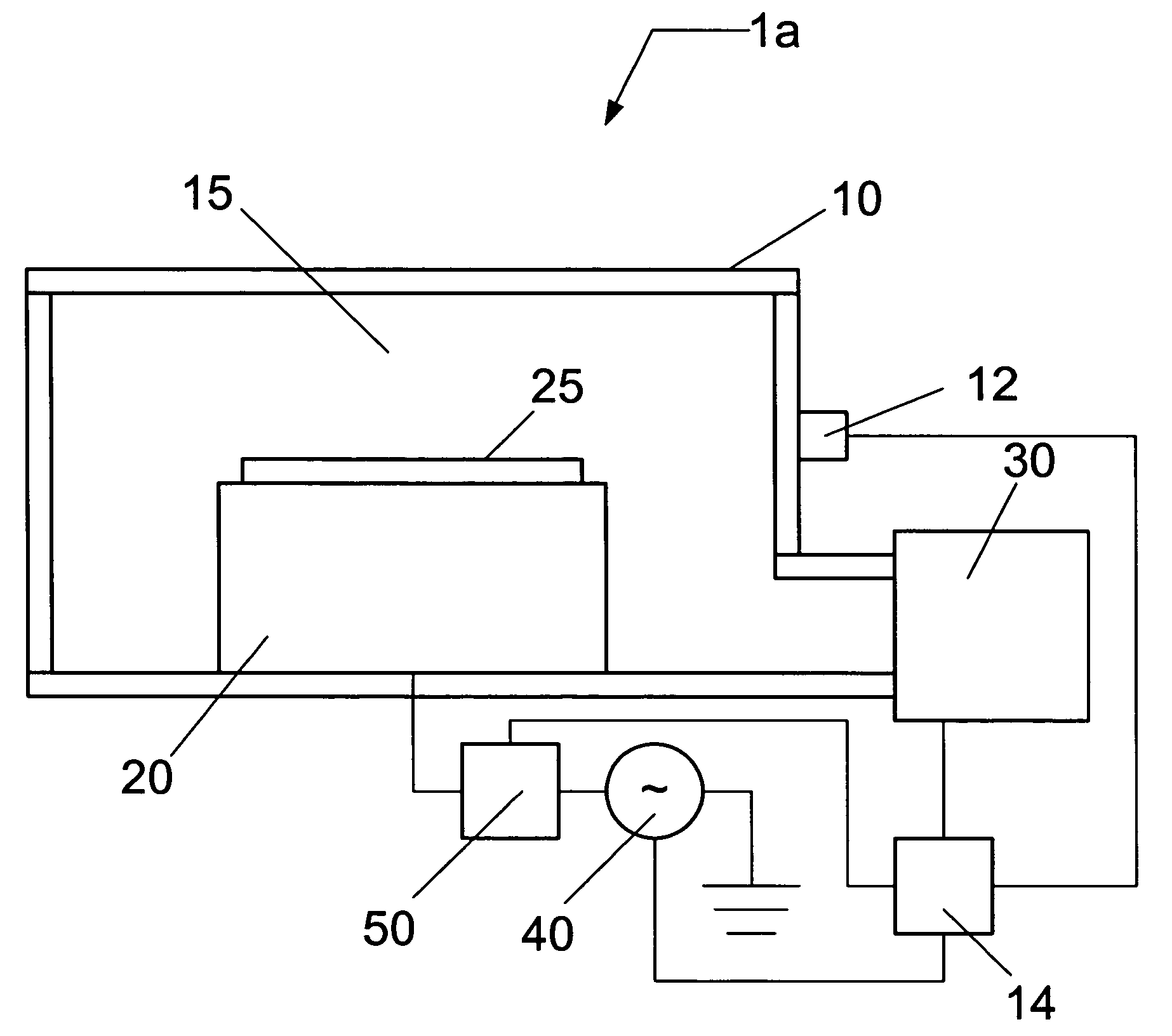
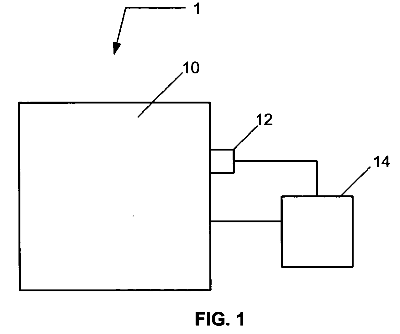
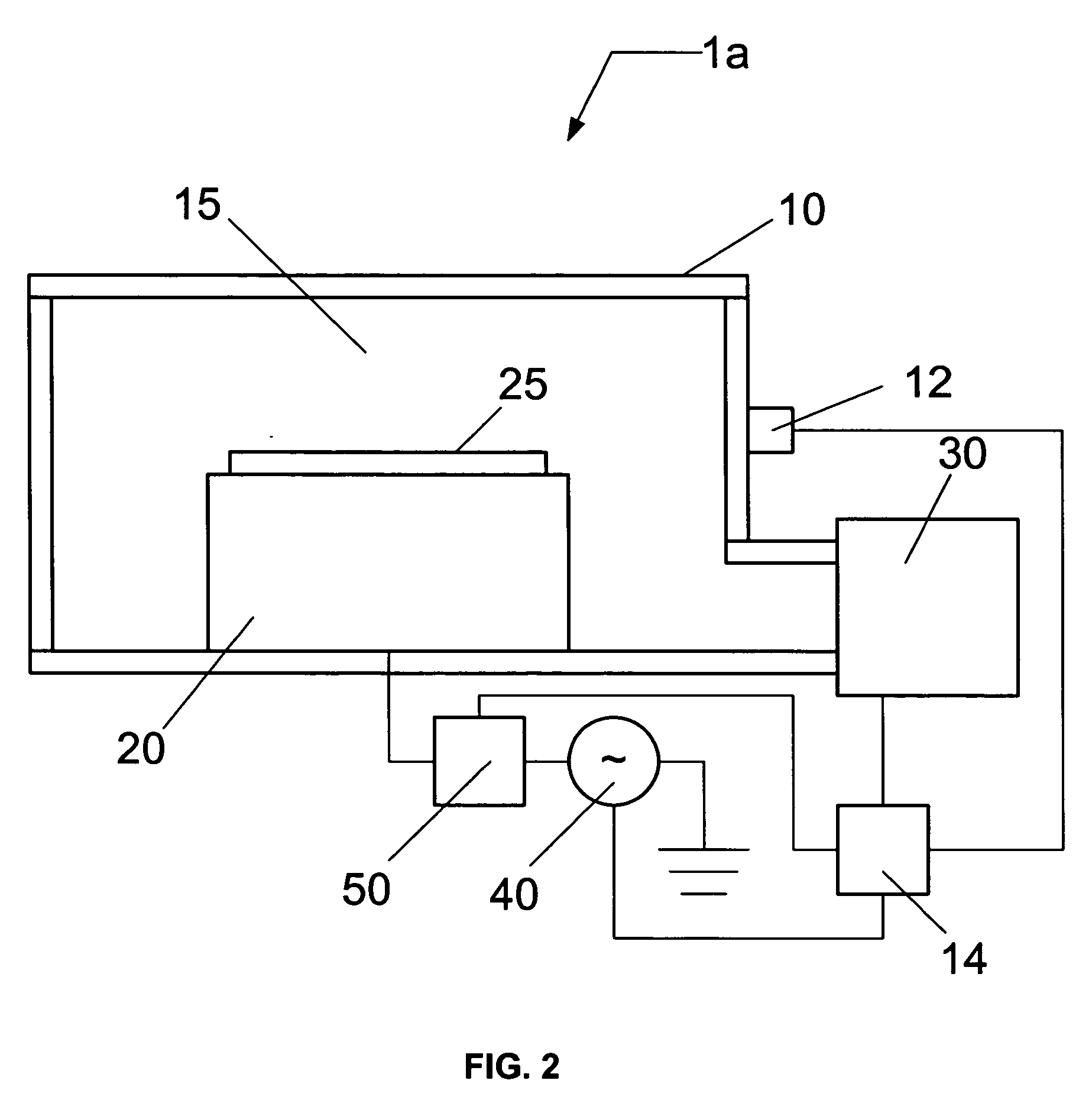
[0029] According to one embodiment, a plasma processing system 1 is depicted in FIG. 1, comprising a plasma processing chamber 10, a diagnostic system 12 coupled to the plasma processing chamber 10, and a controller 14 coupled to the diagnostic system 12 and the plasma processing chamber 10. The controller 14 ...
PUM
| Property | Measurement | Unit |
|---|---|---|
| Length | aaaaa | aaaaa |
| Pressure | aaaaa | aaaaa |
| Thickness | aaaaa | aaaaa |
Abstract
Description
Claims
Application Information