Manufacturing method of die for optical element molding

a manufacturing method and technology for optical elements, applied in the field of manufacturing methods for manufacturing dies for optical elements, can solve the problem and achieve the effect of very low possibility of broken parts

Inactive Publication Date: 2005-11-03
KONICA MINOLTA OPTO
View PDF6 Cites 52 Cited by
  • Summary
  • Abstract
  • Description
  • Claims
  • Application Information

AI Technical Summary

Benefits of technology

[0017] One of modes of the present invention is a manufacturing method of the die for optical element molding, and which is characterized in that it has: a process for forming the first film layer of the amorphous alloy having the super-cooling liquid phase formed of a predetermined composition on the master transfer surface of the master die for molding the molding transfer surface of the die for optical element molding; a process for heating the first film layer (called also a heating press process) more than the glass transition point of the amorphous alloy having the super-cooling liquid phase while pressing under the condition that the surface of the first film layer and the shifted surface of the base material of the die for optical element molding are faced; and

Problems solved by technology

When the shape of the master transfer surface of the master die is transferred onto the transferred surface of the die, because the dynamic transfer by the

Method used


Image

  • Manufacturing method of die for optical element molding
  • Manufacturing method of die for optical element molding
  • Manufacturing method of die for optical element molding

Examples


example

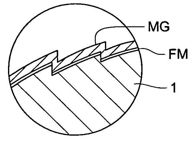
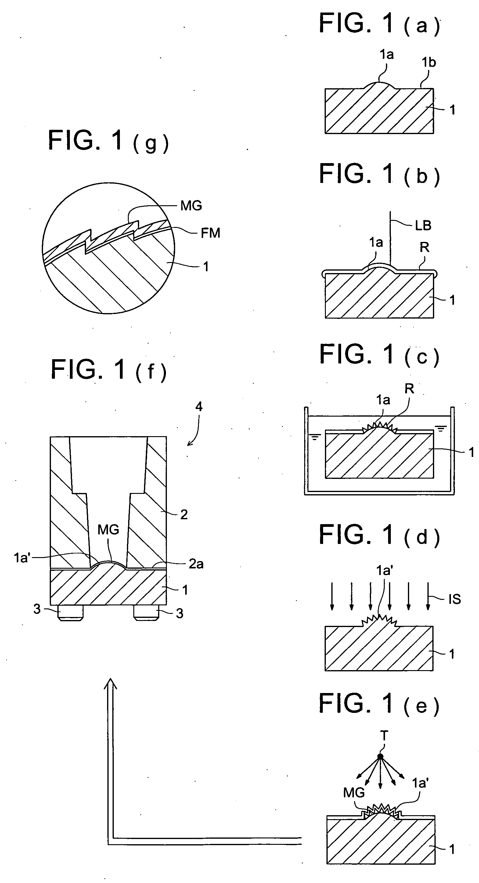
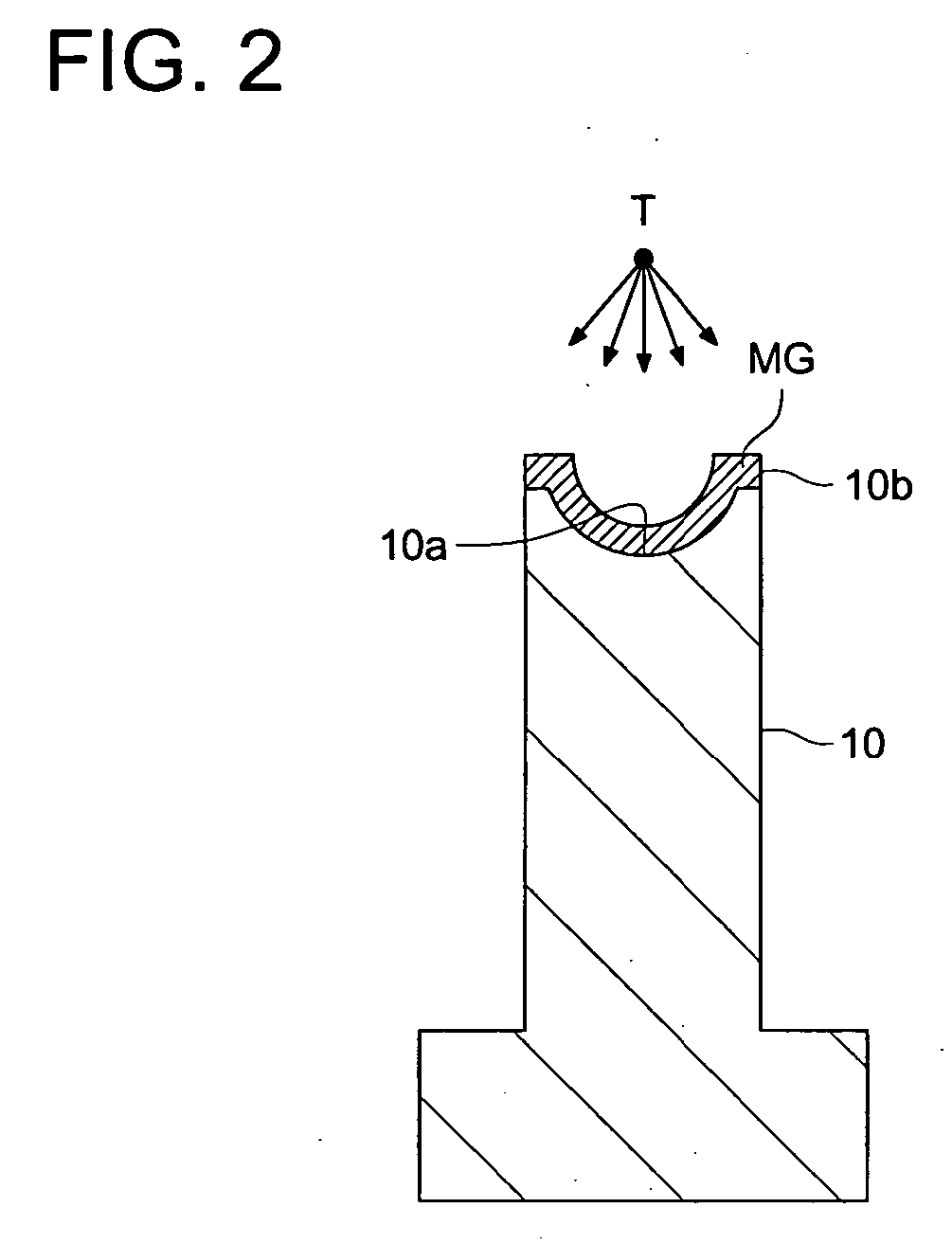
[0133] In contrast to this, an Example carried out by the present inventors will be described below. Initially, 5 base materials of the master die and metallic mold are manufactured in the same manner as the comparative example. After that, also on the base material of the metallic mold, simultaneously with the master transfer surface of the master die, the amorphous alloys having the super-cooling liquid phase Tg-Tx between 295-395° C., are respectively film-formed by the spattering film formation apparatus in the thickness of 0.02, 10, 50, 100, 500 μm. After that, the master transfer surface of the master die on which the amorphous alloy film layer is formed and the base material (or, base material of the metallic mold on which the amorphous alloy film layer having the super-cooling liquid phase is formed) are oppositely arranged, and in the atmosphere (about 100 Pa) substituted by He-gas, when it is heated to 310° C. which is more than the glass transition point, and press-molded...


PUM

PropertyMeasurementUnit
Thicknessaaaaaaaaaa
Thicknessaaaaaaaaaa
Temperatureaaaaaaaaaa

Abstract

The invention relates to a manufacturing method of a die for molding an optical element. The manufacturing method comprising: forming the first film layer of an amorphous allow having a super-cooling liquid phase onto a master transfer surface of a master die for molding a molding transfer surface of the die; heating the first film layer more than a glass transition point of the amorphous alloy having the super-cooling liquid phase while a surface of the first film layer and a transferred surface of a base material of the die being faced and pressed; and peeling the first film layer from the master die and transferring the first film layer onto the base material of the die to form the molding transfer surface of the die.

Description

TECHNICAL FIELD [0001] The present invention relates to a manufacturing method for manufacturing a die for optical element molding by using a master die. BACKGROUND ARTS [0002] According to the manufacturing method of a molding die of a plastic optical element which is conventionally generally conducted, a blank (primary product) is manufactured by, for example, steel or stainless steel, and an alloy of an amorphous-like nickel and phosphorous is filmed in the thickness of about 100 μm by a chemical plating, which is called electroless plating, on it, and this plating layer is cutting processed by a diamond tool in an ultra-precise processing machine, and a highly accurate optical surface transfer surface for molding the optical surface of the optical element is obtained. [0003] According to such a method of the conventional technology, because shapes of parts are created basically by the mechanical processing, the part accuracy is easily increased to near the movement accuracy of t...

Claims


Application Information

Patent Timeline
IPC IPC(8): B22D23/00B29C33/38B29C33/42B29D11/00C03B11/00C03B11/08C23C14/00C23C16/00G02B3/00G02B5/18
CPCB29C33/424C03B11/082C03B11/086C03B2215/16C03B2215/17C03B2215/412C03B2215/22C03B2215/24C03B2215/32C03B2215/34C03B2215/20Y02P40/57C12G3/08
Inventor YUASA, SEIJIHOSOE, SHIGERU
Owner KONICA MINOLTA OPTO
Why Eureka
Try Eureka