Material for contact etch layer to enhance device performance

a contact etch layer and material technology, applied in the field of thin films, can solve the problems of not being able to provide the conventional film and method of producing nitride liners and other films have not necessarily provided all the characteristics that may be desirable for field effect transistors (fets) and other applications, so as to achieve better conformity and load

Inactive Publication Date: 2005-11-03
IBM CORP
View PDF19 Cites 21 Cited by
  • Summary
  • Abstract
  • Description
  • Claims
  • Application Information

AI Technical Summary

Benefits of technology

[0064] In the present invention, films may be deposited in a thickness as desired, with a preferred range of film thickness being about 50 to 1,000 angstroms. The present invention further provides for variability of the film thickness for giving a desired stress level. For example, a nitride film thickness can be varied to provide different stress levels as desired. In setting the nitride thickness, the application (such as use as an etch-stop liner) is considered.
[0065] For example, for successfully using an inventive film (such as a BTBAS film) as an etch-stop liner, the spacer nitrides should be carefully selected with regard to thickness and stress, taking into account that the improvement in stress given by films according to the invention compared to conventional films is due to the exertion of tensile stress at the corner of the gate. That is, because the improvement is due to the exertion of tensile stress at the corner of the gate, if the spacer is too thick, or has too high a stress, the effect of the inventive film (such as a BTBAS film) would be minimized. Accordingly, the spacer nitrides should be selected so as not to be too thick or to provide too high a stress for the particular application, when an inventive film (such as a BTBAS film) is used as an etch-stop liner.
[0066] Inventive films (such as BTBAS films) have advantageous applications for tensile stress production, providing a spacer, and other applications known for RTCVD SiH4 films or PECVD films for spacer formation. Advantageously, the present invention provides spacers (such as BTBAS spacers) that give better conformity and loading effect than conventional nitride films.
[0067] Some inventive examples are given below, without the invention being limited to such examples.

Problems solved by technology

However, the question of satisfying a particular application is multi-variate and may be relatively complicated.
However, the conventional films and methods for producing nitride liners and other films have not necessarily provided all of the characteristics that may be desirable for field effect transistors (FETs) and other applications.
For example, conventionally, nitride films used as a nitride liner have not been able to provide as much stress as would be desirable while balancing other needed characteristics.
Nor are there adequately simple, feasible production methodologies for making films and semiconductor devices (such as FETs) to have desired characteristics.

Method used


Image

  • Material for contact etch layer to enhance device performance
  • Material for contact etch layer to enhance device performance
  • Material for contact etch layer to enhance device performance

Examples


##ventive example 1

INVENTIVE EXAMPLE 1

[0068] A film (i.e., a nitride film) was deposited by reacting BTBAS and NH3 in a single wafer reactor. A process condition is selected which gives a carbon concentration of 3 to 15 atomic %.

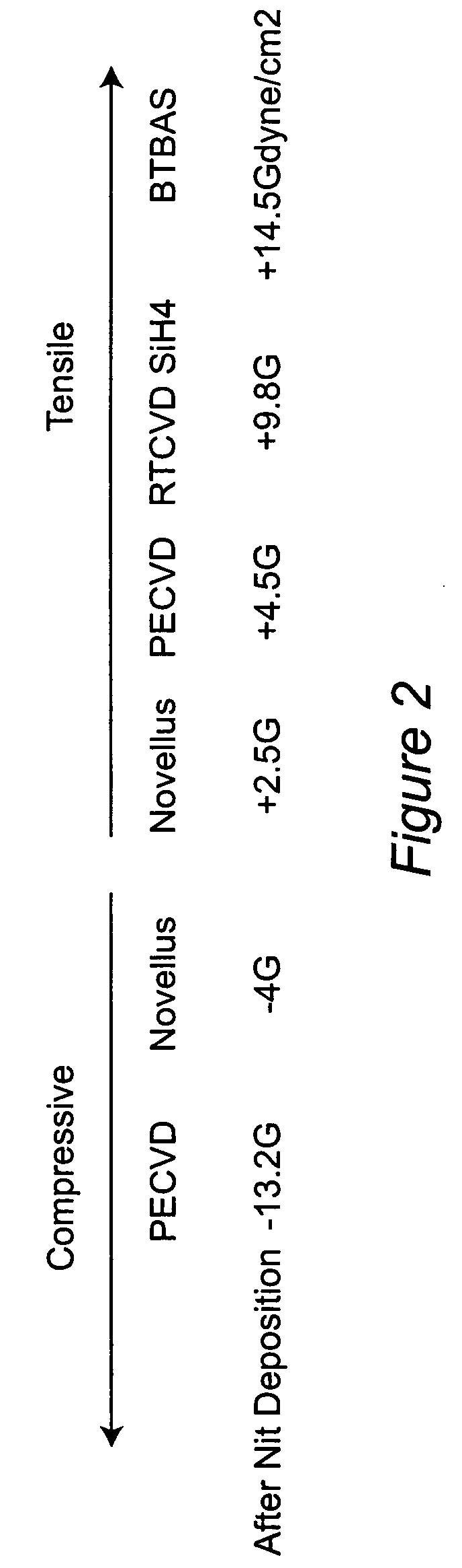
[0069] Device data was obtained that shows the drive current improvement compared to conventional films. FIGS. 3 and 4 show the electrical characteristics of the nFET and pFET. BTBAS nitride film can provide higher NFET drive current compared with devices with PECVD Tensile Nit film (and PECVD Compressive Nit film). There is also no degradation on the pFET drive current, for the film according to the inventive example. The nFET drive current improvement is dependent on the local strain, hence the device geometry and nitride thickness. In general, for a long width nFET device, BTBAS with 500 A in thickness can provide 8% nFET current improvement, with 750 A BTBAS giving extra 3% current improvement. There is also no degradation on the pFET drive current.

[0070] The FIG. 5 Iodl...

##ventive example 2

INVENTIVE EXAMPLE 2

[0071] In an RTCVD process, BTBAS and NH3 are reacted, under the following conditions:

Carbon concentration:˜6 to 10%Temperature650° C.Pressure140 torrDilane, disilane, hexachloro disilane?None

Films of thickness 500 or 750 angstroms are formed. Other film thicknesses may be formed.


PUM

PropertyMeasurementUnit
temperatureaaaaaaaaaa
thicknessaaaaaaaaaa

Abstract

Stress level of a nitride film is adjusted as a function of two or more of the following: identity of a starting material precursor used to make the nitride film; identity of a nitrogen-containing precursor with which is treated the starting material precursor; ratio of the starting material precursor to the nitrogen-containing precursor; a set of CVD conditions under which the film is grown; and/or a thickness to which the film is grown. A rapid thermal chemical vapor deposition (RTCVD) film produced by reacting a compound containing silicon, nitrogen and carbon (such as bis-tertiary butyl amino silane (BTBAS)) with NH3 can provide advantageous properties, such as high stress and excellent performance in an etch-stop application. An ammonia-treated BTBAS film is particularly excellent in providing a high-stress property, and further having maintainability of that high-stress property over repeated annealing.

Description

BACKGROUND OF THE INVENTION [0001] 1. Field of the Invention [0002] The present invention generally relates to integrated circuit manufacture, and more particularly to thin films and their production and their uses in conferring advantages upon the semiconductor devices being manufactured, especially in rapid thermal chemical vapor deposition (RTCVD) processes. [0003] 2. Background Description [0004] Conventionally, various films have been produced for use in circuit manufacture (such as making transistors), in a variety of types of chemical vapor deposition (CVD) processes. Examples of the various CVD processes are low pressure chemical vapor deposition (LPCVD), plasma-enhanced chemical vapor deposition (PECVD), high density plasma chemical vapor deposition (HDPCVD), rapid thermal chemical vapor deposition (RTCVD), cyclic deposition (CLD), atomic layer deposition (ALD), and mixed deposition (MLD) (i.e., a mixture of CLD and ALD); etc. The respective deposition processes differ sign...

Claims


Application Information

Patent Timeline
Patent Type & Authority Applications(United States)
IPC IPC(8): C23C16/34H01L21/768H01L21/318H01L21/469H01L29/78
CPCC23C16/345H01L29/7843H01L21/3185H01L21/02274H01L21/02271H01L21/0217
Inventor CHAKRAVARTI, ASHIMA B.NARASIMHA, SHREESHCHAN, VICTORHOLT, JUDSONCHAKRAVARTI, SATYA N.
Owner IBM CORP
Why Eureka
Try Eureka