

Chemical mechanical polishing pad, manufacturing process thereof and chemical mechanical polishing method for semiconductor wafers
a technology of chemical mechanical polishing pad and manufacturing process, which is applied in the direction of manufacturing tools, grinding devices, lapping machines, etc., can solve the problems of difficult to obtain a polishing pad, reduced or non-uniform polishing efficiency of the polishing pad, and inefficient polishing time, etc., to achieve the effect of not reducing the polishing efficiency
- Summary
- Abstract
- Description
- Claims
- Application Information
AI Technical Summary
Benefits of technology
Problems solved by technology
Method used
Image

Examples
example 1
1. Manufacture of Polishing Pad
[0129] 1-1. Production of Surface Treated β-cyclodextrin
[0130] 100 parts by weight of β-cyclodextrin (manufactured by Yokohama International Bio Research Laboratory Co., Ltd., trade name of Dexy Pearl β-100, average particle diameter of 20 μm) as water-soluble particles was fed to a mixer (Super Mixer SMZ-3SP of Kawata Co., Ltd.), 0.5 part by weight of γ-aminopropyltriethoxysilane (manufactured by Nippon Unica Co., Ltd., trade name of A-1100) was sprayed on the water-soluble particles for 5 minutes under agitation at 400 rpm, and the coated water-soluble particles were further stirred at 400 rpm for 2 minutes. Thereafter, the extracted particles were dried by heating in a vacuum drier set at 130° C. until the water content became 5,000 ppm or less to obtain surface treated β-cyclodextrin.
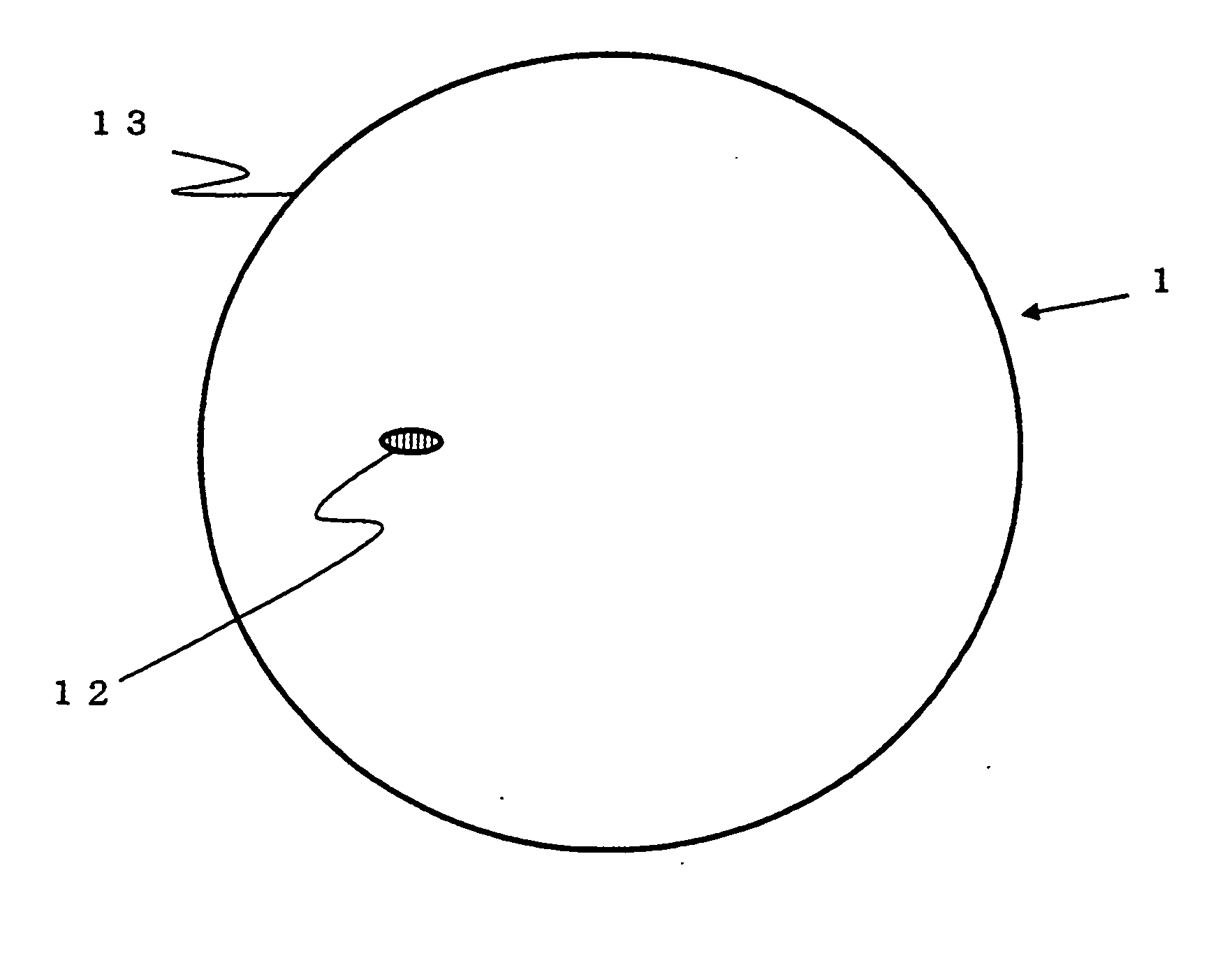
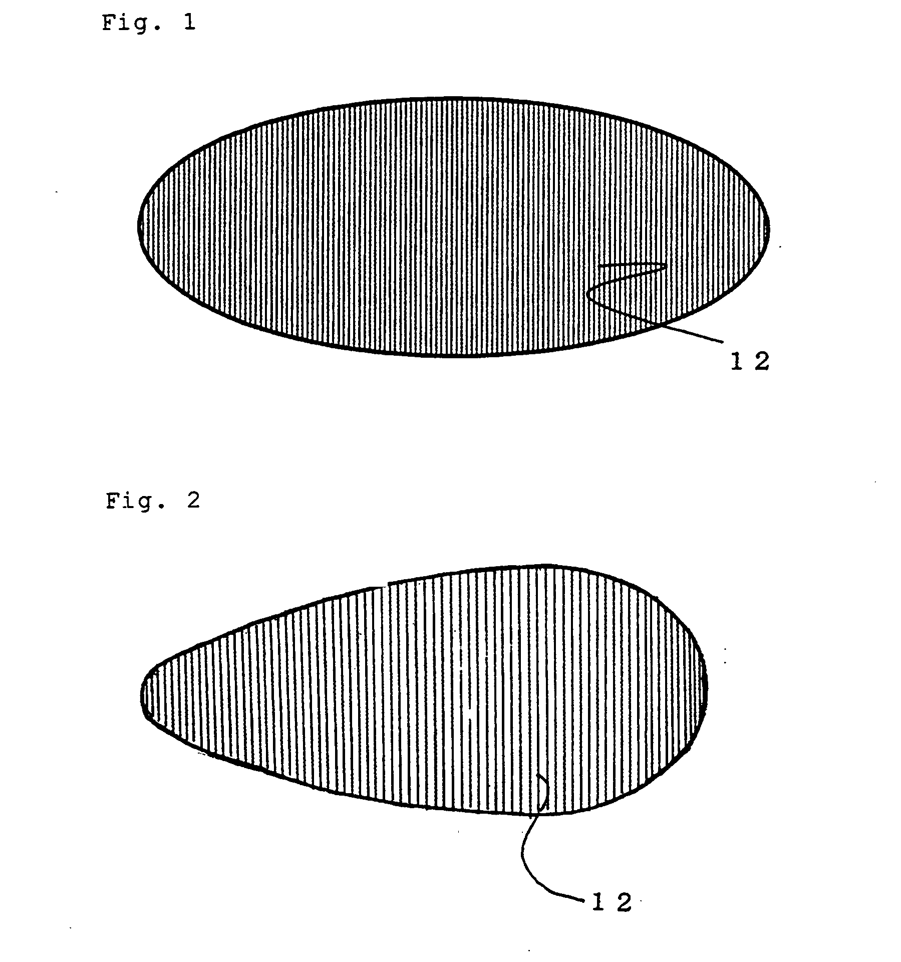
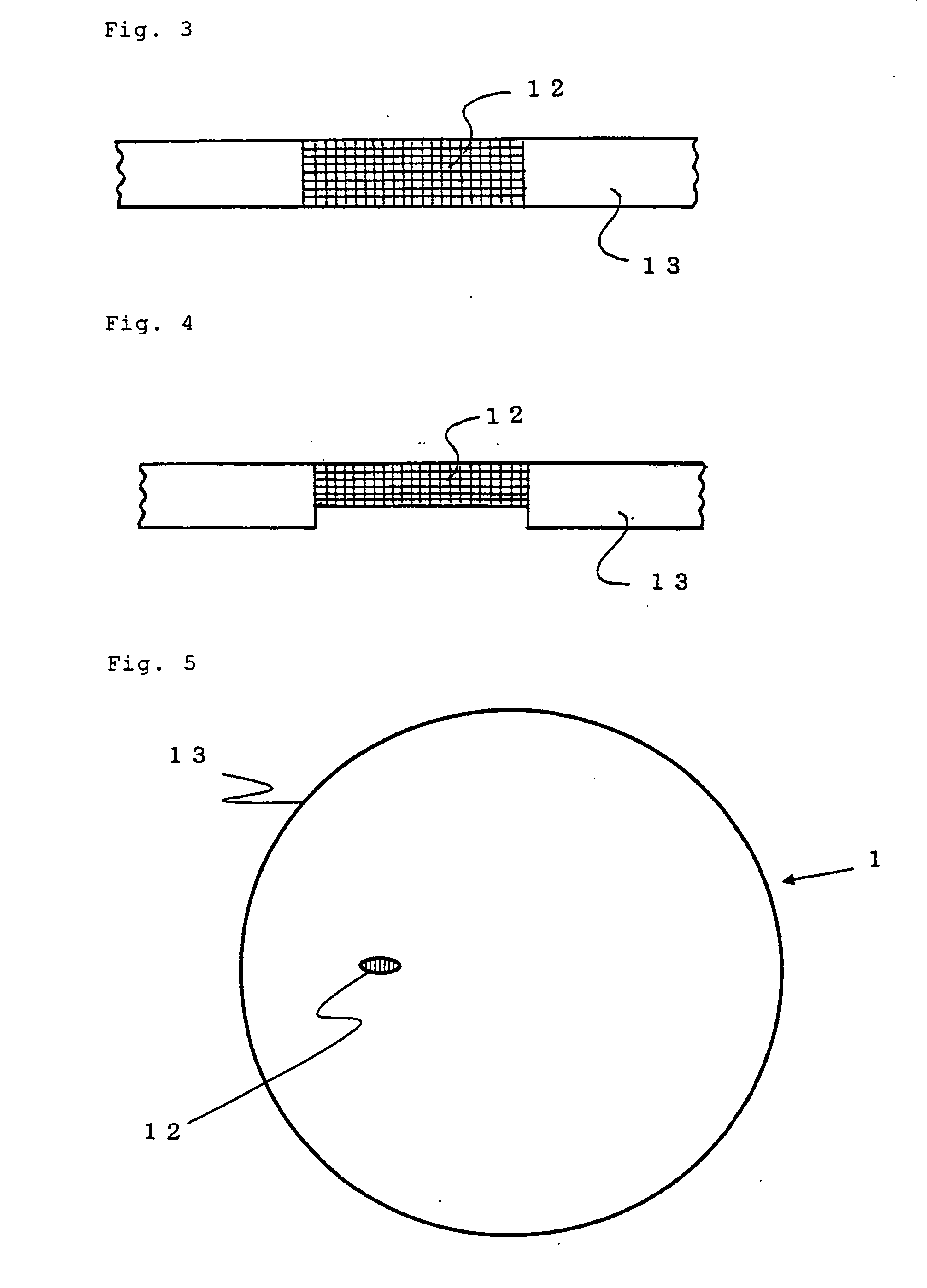
[0131] 1-2. Manufacture of Polishing Pad Having an Elliptic Hole
[0132] 66.5 vol % of 1,2-polybutadiene (manufactured by JSR Corporation, trade name of JSR RB830) ...
examples 2
Manufacture of Polishing Pad
[0152] 64 volt of 1,2-polybutadiene (manufactured by JSR Corporation, trade name of JSR RB830) and 16 volt of a styrene-butadiene elastomer (manufactured by JSR Corporation, trade name of JSR TR2827) both of which would be crosslinked to become a matrix material and 20 volt of the surface treated β-cyclodextrin produced in “1-1.” of Example 1 as a water-soluble substance were kneaded together by an extruder heated at 160° C. Thereafter, Percumyl D40 (trade name, manufactured by NOF Corporation, containing 40% by mass of dicumyl peroxide) was added in an amount of 0.4 part by mass (equivalent to 0.16 part by mass in terms of pure dicumyl peroxide) based on 100 parts by mass of the total of 1,2-polybutadiene and styrene-butadiene elastomer and further kneaded with the above kneaded product to carry out a crosslinking reaction at 160° C. in a press metal mold for 7 minutes to obtain a disk-like molded product having a diameter of 790 mm and a thickness of ...
examples 3
Manufacture of Polishing Pad
[0155] 80 volt of 1,2-polybutadiene (manufactured by JSR Corporation, trade name of JSR RB830) which would be crosslinked to become a matrix material and 20 volt of the surface treated β-cyclodextrin produced in “1-1.” of Example 1 as a water-soluble substance were kneaded together by an extruder heated at 160° C. Thereafter, Percumyl D40 was added in an amount of 0.8 part by mass (equivalent to 0.32 part by mass in terms of pure dicumyl peroxide) based on 100 parts by mass of 1,2-polybutadiene and further kneaded with the above kneaded product to carry out a crosslinking reaction at 160° C. in a press metal mold for 7 minutes to obtain a disk-like molded product having a diameter of 790 mm and a thickness of 3.2 mm. An elliptic hole (aspect ratio of 10) having a long diameter of 70 mm and a short diameter of 7 mm was formed at a position 195 mm away from the center of the pre-polishing substrate as the center thereof by an end mill of Kato Machinery Co...
PUM
| Property | Measurement | Unit |
|---|---|---|
| Fraction | aaaaa | aaaaa |
| Fraction | aaaaa | aaaaa |
| Fraction | aaaaa | aaaaa |
Abstract
Description
Claims
Application Information