Silicon wafer and method for manufacturing the same

a technology of silicon wafers and wafers, applied in the field of silicon wafers, can solve the problems of degrading the inside pressure of the oxide film, increasing the bulk micro defect, and increasing the leakage current, so as to increase the precipitation oxygen and remove the slicing damag

Inactive Publication Date: 2005-11-10
LG SILTRON
View PDF6 Cites 23 Cited by
  • Summary
  • Abstract
  • Description
  • Claims
  • Application Information

AI Technical Summary

Benefits of technology

[0021] Preferably, the preparing of the silicon wafer includes the steps of: dipping a seed crystal in a silicon melt and growing a single-crystalline silicon by pulling up the seed crystal while adjusting a crystal growing speed and a temperature gradient along a growing axis at a boundary of solid and liquid phase boundary; slicing the grown single-crystalline silicon into shapes of wafers; and removing slicing damage generated from slicing and rounding sides of the sliced wafer or etching a surface of the sliced wafer; wherein the single-crystalline silicon is grown with nitrogen doped in concentration ranging from about 1×10¹² atoms / cm3 to about 1×10¹⁴ atoms / cm3 so as to increase precipitated oxygen.

Problems solved by technology

Further, manufacturers have been required to increase the bulk micro defect “BMD” density which consists primarily of oxygen precipitates and the bulk or oxidation stacking fault in the bulk area beneath the active region of the resulting device.
When the oxygen precipitates are on the surface of the wafer, they increase leakage current and degrade an oxide film inside-pressure, which are both disadvantageous characteristics for a semiconductor device.
However, in this case, the oxygen precipitates are reduced in a bulk zone, and therefore the BMD density is also low.
Also manufacturing pure single-crystalline silicon is costly.
While, this method has improved techniques over the pure single-crystalline silicon manufacturing method discussed above and the annealed wafer manufacturing method discussed below, it is very costly.
However, current annealing techniques require numerous adjustments to the gas atmosphere, temperature ramp-up / down rates and heat treatment temperatures / times, all of which make control of the process very difficult, costly and unreliable.
Consequently, current annealing processes generate defects such as slip during the high temperature processes, or the annealed wafer can't be manufactured with a uniform and sufficient non-defect zone and high BMD density.

Method used


Image

  • Silicon wafer and method for manufacturing the same
  • Silicon wafer and method for manufacturing the same
  • Silicon wafer and method for manufacturing the same

Examples


Embodiment Construction

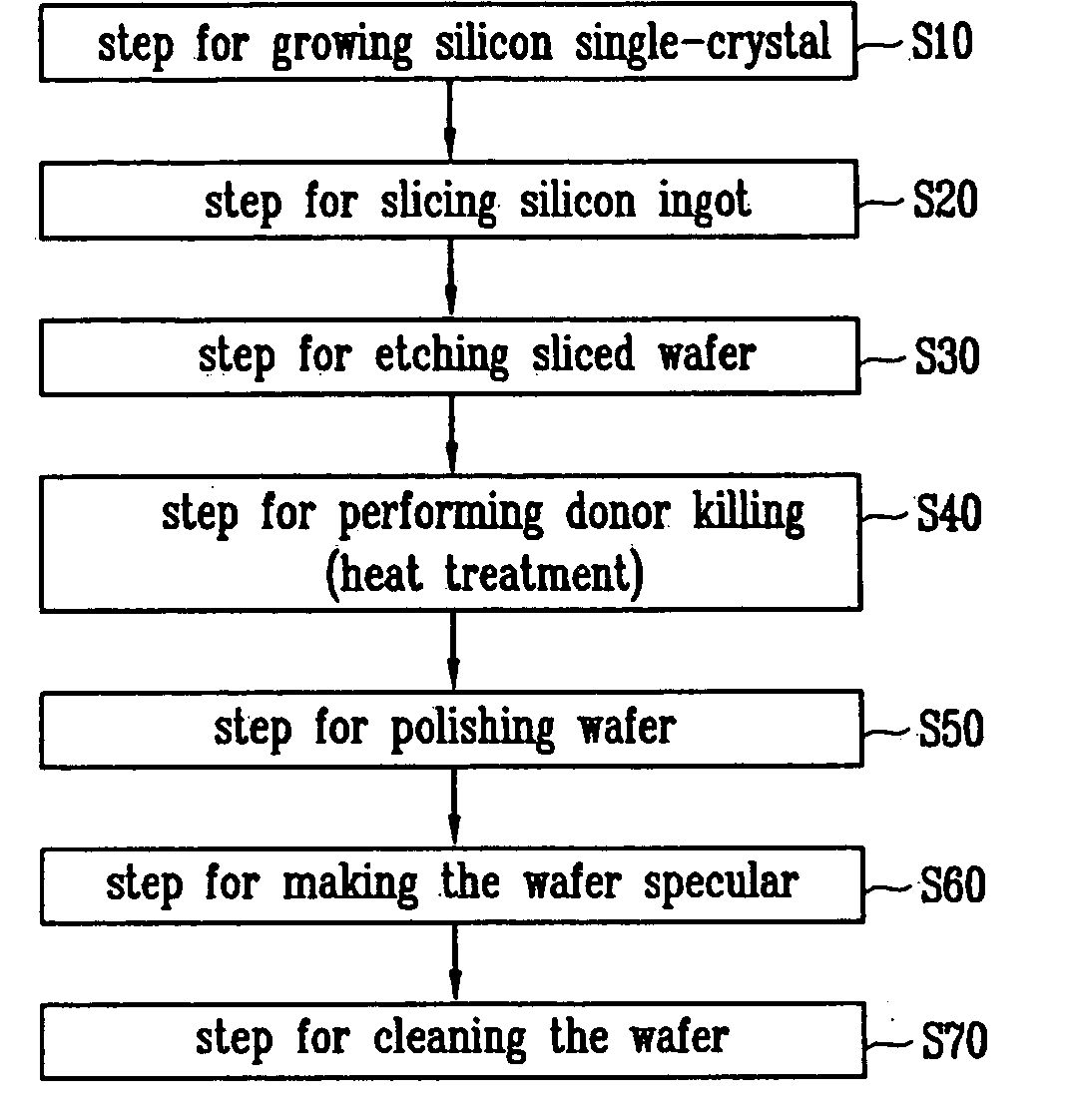
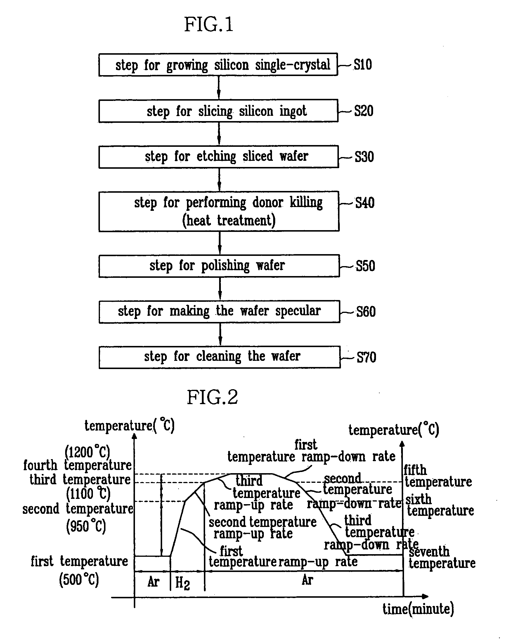
[0047] Disclosed methods for manufacturing silicon wafers will now be described in detail with reference to the accompanying drawings.

[0048] Referring to FIG. 1, a single-crystalline silicon is grown using a Czochralski CZ method (S10). After dipping a seed crystal into a silicon melt, the crystal is slowly pulled and grown. The nitrogen is to be doped in a silicon single-crystalline ingot during the crystal growing. The nitrogen doping concentration is preferably about 1×10¹² atoms / cm3 through 1×10¹⁴ atoms / cm3.

[0049] Next, the ingot is sliced into shapes of wafer (S20).

[0050] Slicing damages occurred in performing the slicing process are removed, and an etching process is carried out for etching a surface or rounding a side of the sliced wafer (S30).

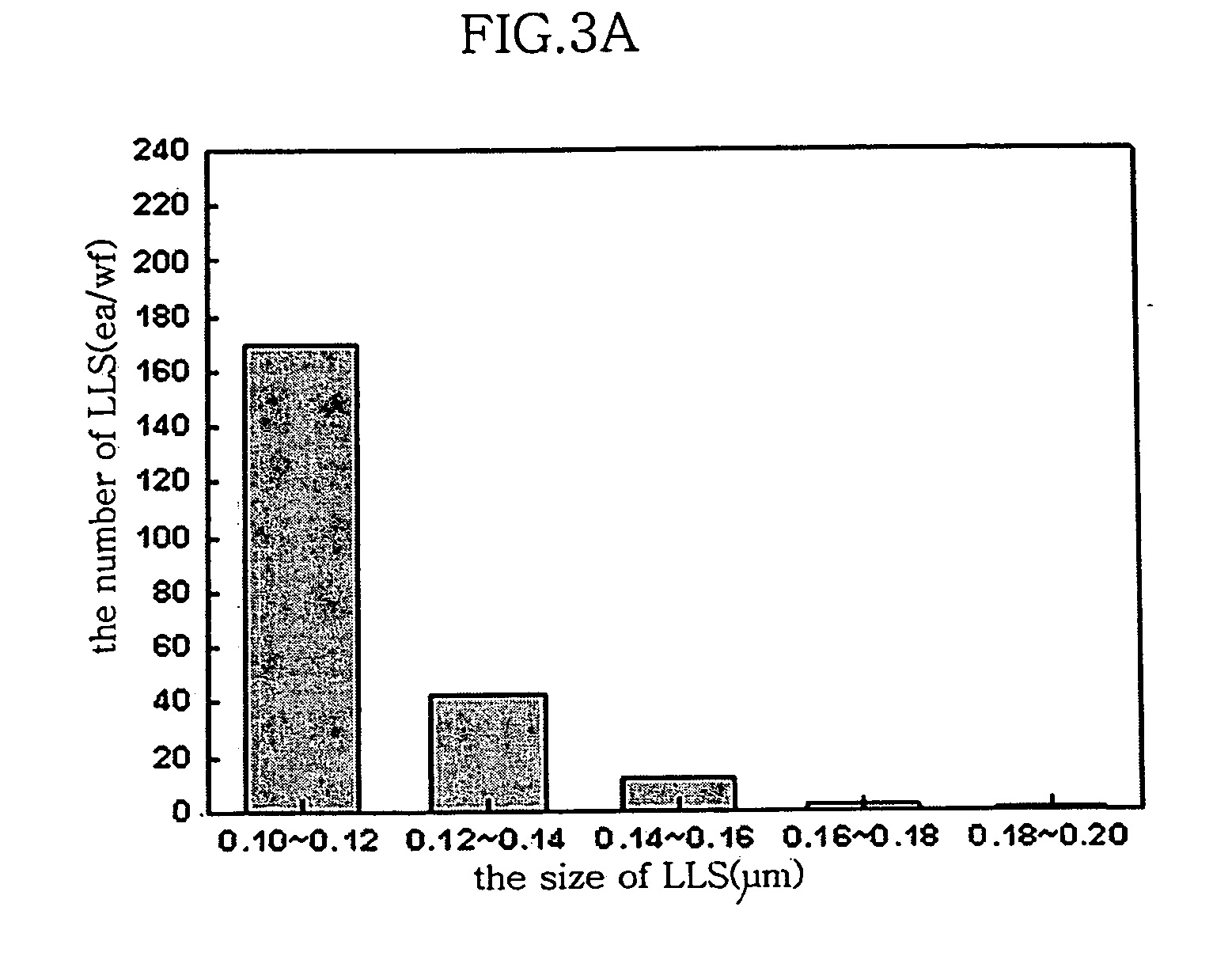
[0051] A donor killing process is the performed (S30), in which oxygen is generated from a crystal growing step included in a silicon wafer which includes oxygen precipitates from a heat treatment process. That is, approximately 101...


PUM

PropertyMeasurementUnit
depthsaaaaaaaaaa
temperatureaaaaaaaaaa

Abstract

A method for manufacturing a high quality annealed wafer which has both a uniform and high density bulk micro defect (BMD) in a bulk zone disposed between front and rear denuded zones (DZ), which increases the effect of gettering metal impurities such as Fe, Cu and etc., and which provides a defect free zone in the active region of device.

Description

BACKGROUND [0001] 1. Technical Field [0002] A silicon wafer and a method for manufacturing the same are disclosed. The disclosed wafer has a high density and uniform bulk micro defect (BMD) concentration in a bulk area of the wafer disposed between front and rear denuded zones (DZ). [0003] 2. Discussion of the Related Art [0004] As semiconductor devices become ultra-minute with sizes under 0.1 μm and more highly integrated, the silicon wafers from which these devices are made have become larger, in excess of 300 mm. While the development of large wafers provides numerous advantages, defects in the large wafers must be avoided. [0005] Specifically, manufacturers are required to provide a “non-defect” layer in an active region of the wafer or the resulting semiconductor device. Manufacturers have also been required by customers to effectively remove impurities such as metal particles that can be generated during the manufacturing process. Further, manufacturers have been required to i...

Claims


Application Information

Patent Timeline
Patent Type & Authority Applications(United States)
IPC IPC(8): H01L21/322C30B15/00C30B33/00H01L21/02
CPCC30B29/06H01L21/3225C30B33/00H01L21/322
Inventor YOON, SUNG HOBAE, SO IKMUN, YOUNG HEE
Owner LG SILTRON
Why Eureka
Try Eureka