Organic light emitting device and method of fabricating the same

a light emitting device and organic technology, applied in the field of organic light emitting devices, can solve the problems of low light output, low light output, and difficulty in manufacturing large-sized passive matrix organic light emitting displays, and achieve the effect of not degrading the brightness of the display

Inactive Publication Date: 2005-11-10
SAMSUNG SDI CO LTD
View PDF3 Cites 27 Cited by
  • Summary
  • Abstract
  • Description
  • Claims
  • Application Information

AI Technical Summary

Benefits of technology

[0024] The present invention provides, for example, a top emitting organic light emitting is device and method of fabricating the same, in which galvanic phenomena are prevented at interfaces between a transparent electrode material and a metal material, without degrading brightness of the display.

Problems solved by technology

However, the passive matrix organic light emitting device has high power consumption and it is difficult to manufacture large-sized passive matrix organic light emitting displays.
Furthermore, the aperture ratio degrades as the number of wirings increases.
However, because there is no suitable single material so far that satisfies such characteristics, the reflecting electrode is generally fabricated in a multi-layer structure in which a separate reflecting layer is formed and an electrode material having a different conductivity is formed thereon.
The potential difference between the two metals may cause corrosion at point of contact of the two metals when the two metals are exposed to a corrosive solution.
In particular, considering that aluminum, an alloy thereof, or the like (used for the reflecting layer) corrodes rapidly to easily form a metal oxide layer 110c such as Al2O3 even when exposed to the air, the formation of the metal oxide layer 110c due to galvanic corrosion can be a very serious problem.
In particular, if some of the chemical substances remain at the interface between the transparent electrode layer 10b and the reflecting layer 110a, severe problems can occur.
Galvanic corrosion can spread along the interface between the transparent electrode layer 110b and the reflecting layer 110a and can rapidly increase contact resistance between the electrodes, resulting in an unstable distribution of the resistance.
As a result, when the top emitting organic light emitting device operates, brightness non-uniformity can occur in which some pixels are bright while some are dark.
However, when the pixel electrode in the above-referenced patent is applied to the top emitting organic light emitting device, the MoW is formed to a thickness of 3000 Å. This lowers the reflectivity of light emitted from the organic layer, and in turn the lowered reflectivity degrades the brightness of the top emitting organic light emitting device.

Method used


Image

  • Organic light emitting device and method of fabricating the same
  • Organic light emitting device and method of fabricating the same
  • Organic light emitting device and method of fabricating the same

Examples


Embodiment Construction

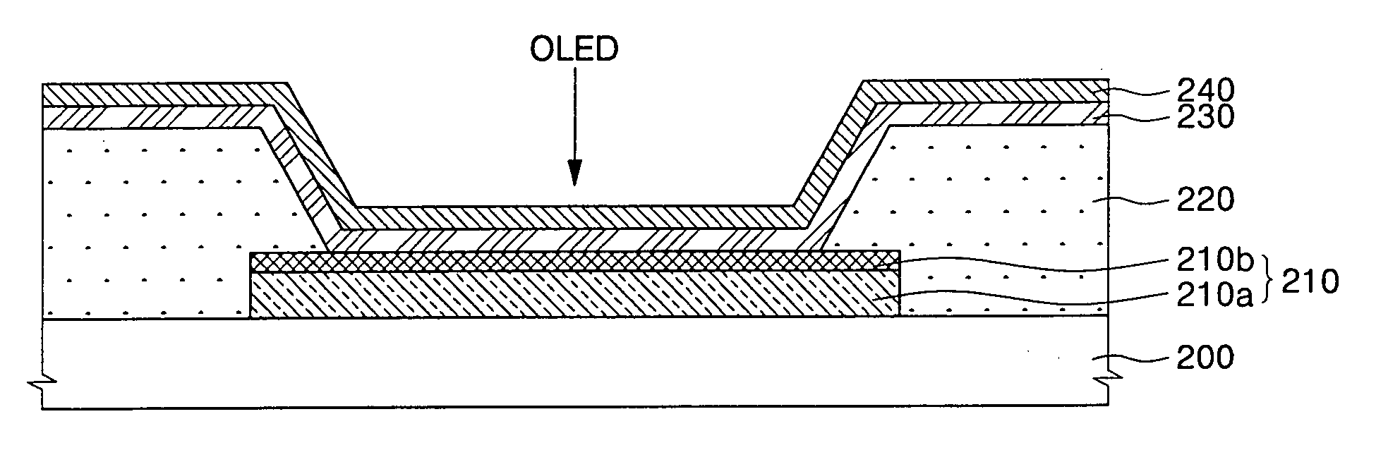
[0034] As shown in FIG. 3A, a reflecting layer 210a may be formed (of a metal material having excellent reflection efficiency) on an insulating substrate 200. The reflecting layer 210a may be formed of a material having excellent reflection efficiency and having an oxidation-reduction potential (a.k.a., Redox Potential) difference of about 0.3 or less with respect to a pixel electrode. This may help to prevent galvanic reaction with the pixel electrode that is to be formed. More preferably, the reflecting layer 210a may be formed of an Al—Ni alloy.

[0035] It is preferable that the Al—Ni alloy used for the reflecting layer 210a be an Al alloy containing nickel (Ni) of about 10% or less.

[0036] The reflecting layer 210a may also be formed by a typical method, such as radio frequency (RF) sputtering, direct current (DC) sputtering, ion beam sputtering, vacuum deposition, or the like.

[0037] Further, either a glass substrate or a plastic substrate may be used as the substrate 200.

[0038...


PUM


Abstract

An organic light emitting device may includes a pixel electrode formed on a substrate and having a reflecting layer and a transparent electrode layer, a pixel defining layer having an opening to expose a portion of the pixel electrode, an organic layer formed on the opening, and an upper electrode formed on an entire surface of the substrate. The reflecting layer may be a material having excellent reflection efficiency and having an oxidation-reduction potential difference of about 0.3 or less with respect to the transparent electrode layer.

Description

CROSS-REFERENCE TO RELATED APPLICATION [0001] This application claims priority to and the benefit of Korean Patent Application No. 2004-32844, filed May 10, 2004, which is incorporated herein by reference in its entirety. BACKGROUND OF THE INVENTION [0002] (a) Field of the Invention [0003] The present invention relates to an organic light emitting device and, more particularly, to an organic light emitting device capable of preventing galvanic reaction in a reflective pixel electrode. [0004] (b) Description of the Related Art [0005] Generally, an organic light emitting device is a light emitting device that emits light when electrons and holes are injected from an electron injection electrode (cathode) and a hole injection electrode (anode) to an emission layer and excitons created by recombination of the injected electrons and holes transition from an excited state to a ground state. [0006] The use of this principle eliminates the need for a separate light source that was necessary...

Claims


Application Information

Patent Timeline
Patent Type & Authority Applications(United States)
IPC IPC(8): H01L29/08H01L29/18H01L29/20H01L29/22H01L35/24H01L51/00H01L51/50H05B33/24H01L51/52H05B33/10H05B33/12H05B33/14H05B33/26H05B33/28
CPCH01L51/5206H01L2251/5315H01L51/5271H10K50/818H10K50/856H10K2102/3026A61H33/10A61H33/065A61H2201/102A61H2201/0149A61H2201/0228A61H2205/086A61H2205/087A61H2201/025
Inventor SHIN, HYUN-EOK
Owner SAMSUNG SDI CO LTD
Why Eureka
Try Eureka