Semiconductor memory device with ability to adjust impedance of data output driver

a memory device and data output technology, applied in the field of semiconductor memory devices, can solve the problem that the calibration control operation of ocds has not developed

Inactive Publication Date: 2005-11-10
SK HYNIX INC
View PDF4 Cites 13 Cited by
  • Summary
  • Abstract
  • Description
  • Claims
  • Application Information

AI Technical Summary

Benefits of technology

[0049] In accordance with an aspect of the present invention, there is provided a semiconductor memory device for performing an OCD calibration control operation in order to adjust a data output impedance, including: means for decoding an address signal to generate an OCD default control signal, an OCD operation signal and plural data; means fo

Problems solved by technology

However, the above-mentioned OCD calibration control operation is a newly introduced concept by th

Method used


Image

  • Semiconductor memory device with ability to adjust impedance of data output driver
  • Semiconductor memory device with ability to adjust impedance of data output driver
  • Semiconductor memory device with ability to adjust impedance of data output driver

Examples


Embodiment Construction

[0072] Hereinafter, a semiconductor memory device in accordance with the present invention will be described in detail referring to the accompanying drawings.

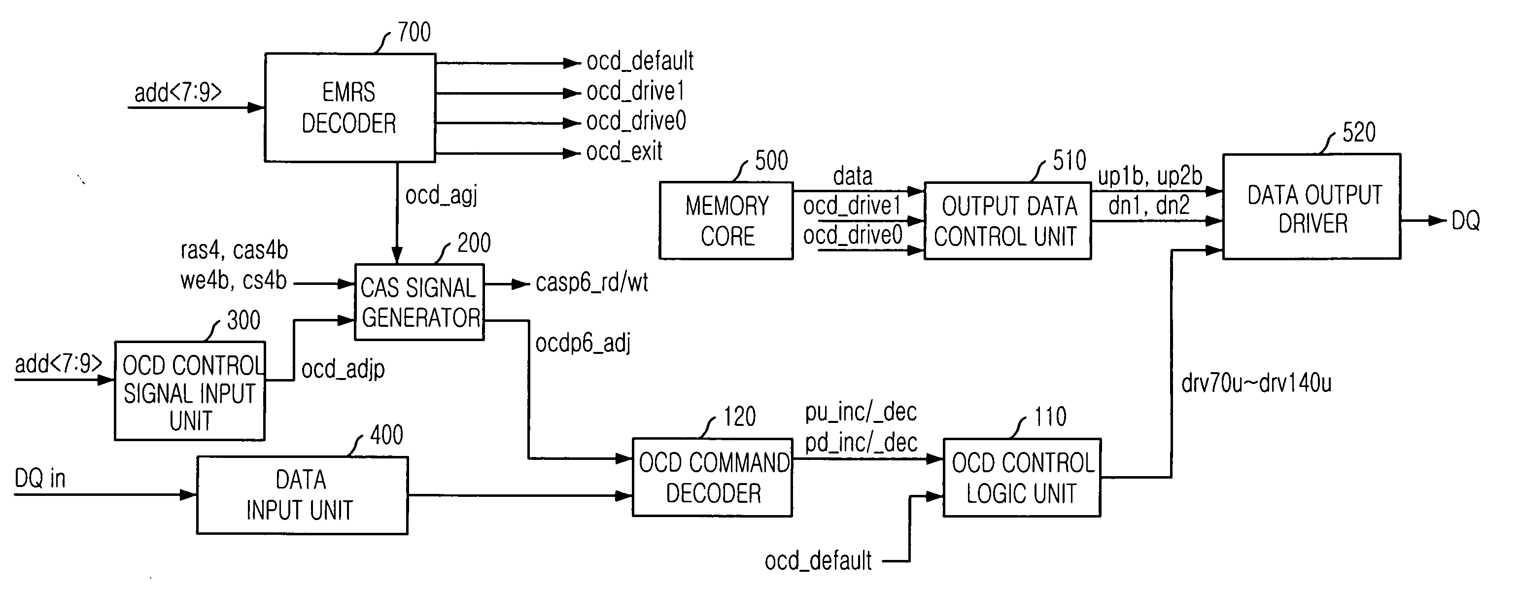
[0073]FIG. 5 is a block diagram showing a semiconductor memory device in accordance with the present invention.

[0074] As shown, the synchronous semiconductor memory device includes an extended mode register set (EMRS) decoder 700, a column address strobe (CAS) signal generator 200, an off chip driver (OCD) control signal input unit 300, a data input unit 400, an OCD command decoder 120, an OCD control logic unit 110, a memory core block 500, an output data control unit 510 and a data output driver unit 520.

[0075] The data input unit 400 latches and aligns plural data inputted through a data input / output pad during a data access operation and the data input unit 400 latches and aligns an OCD control code inputted through the data input / output pad during an OCD calibration control operation. The data output driver 520 outputs ...


PUM


Abstract

A semiconductor memory device for performing an OCD calibration control operation in order to adjust a data output impedance, including: means for decoding an address signal to generate an OCD default control signal, an OCD operation signal and plural data; means for receiving a plural-bit data to generate an OCD control code; means for receiving the OCD control code and the OCD operation signal to generate a plurality of impedance adjustment control signals; and means for receiving the plural data and adjusting the data output impedance in response to the plurality of impedance adjustment control signals.

Description

FIELD OF INVENTION [0001] The present invention relates to a semiconductor memory device; and, more particularly, to a semiconductor memory device capable of adjusting an impedance of a data output driver. DESCRIPTION OF PRIOR ART [0002] A dynamic random access memory (DRAM) has been improved continuously to increase its operational speed. Synchronizing an internal clock signal with an external clock signal is one of methods to improve an operational speed of the DRAM. Particularly, a DRAM which is operated in synchronization with the external clock signal is called a synchronous dynamic random access memory (SDRAM). [0003] The SDRAM performs a data access operation at a rising edge of the external clock signal. That is, the SDRAM can perform the data access operation once within one cycle of the external clock signal. [0004] Such an SDRAM that performs the data access operation once within one cycle of the external clock signal is particularly called a single data rate (SDR) SDRAM....

Claims


Application Information

Patent Timeline
IPC IPC(8): G06F19/00G11C11/407G11C7/10G11C11/40G11C11/401G11C11/4076G11C11/409G11C11/4093H03K3/00
CPCG11C7/1051G11C2207/2254G11C7/1057G11C11/40
Inventor JUNG, HUN-SAM
Owner SK HYNIX INC
Why Eureka
Try Eureka