Tuned microcavity color OLED display

a color oled display and microcavity technology, applied in the direction of discharge tube luminescnet screens, instruments, natural mineral layered products, etc., can solve the problems of reducing the efficiency of light providing, reducing the intensity of one or more of the red, green and blue components of the emission spectrum, and improving the power consumption relative to an rgb device constructed of similar materials, etc., to achieve better color gamut, less color distortion, and color consistency. good

Active Publication Date: 2005-11-10
GLOBAL OLED TECH
View PDF11 Cites 205 Cited by
  • Summary
  • Abstract
  • Description
  • Claims
  • Application Information

AI Technical Summary

Benefits of technology

[0014] It is an advantage of this invention that it provides better color consistency, that is, less color distortion, when viewed at an angle. It is a further advantage of this invention that it provides a better color gamut t

Problems solved by technology

This results in improved power consumption relative to an RGB device constructed of similar OLED materials.
A problem in the application of white OLED devices, when used with color filters, is that the intensity of one or more of the red, green, and blue components of the emission spectrum is frequently lowe

Method used


Image

  • Tuned microcavity color OLED display
  • Tuned microcavity color OLED display
  • Tuned microcavity color OLED display

Examples


example 2 (

INVENTIVE)

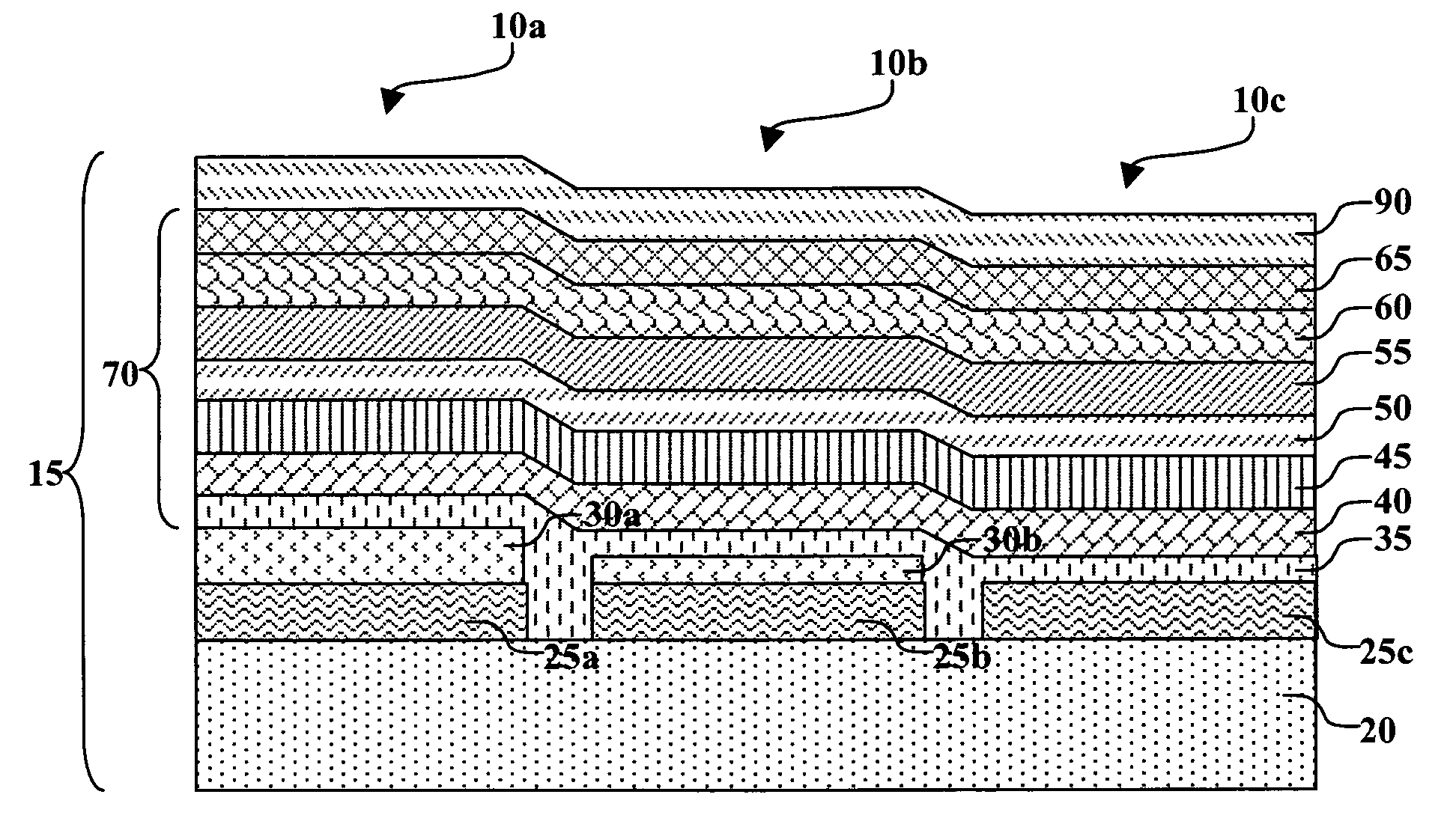
[0201] An inventive color OLED display was constructed in the following manner: [0202] 1. A clean glass substrate was deposited by sputtering with indium tin oxide (ITO) to form a transparent electrode of 85 nm thickness; [0203] 2. The above-prepared ITO surface was treated with a plasma oxygen etch, followed by plasma deposition of a 0.1 nm layer of a fluorocarbon polymer (CFx) as described in U.S. Pat. No. 6,208,075; [0204] 3. The above-prepared substrate was further treated by vacuum-depositing a 240 nm layer of NPB as a hole-transporting layer (HTL); [0205] 4. A 28 nm layer of 20 nm NPB and 8 nm rubrene containing 0.5% TPDPB (above) was vacuum-deposited onto the substrate at a coating station that included a heated graphite boat source to form a red light-emitting layer (red LEL); [0206] 5. A coating of 20 nm of 2-tert-butyl-9,10-bis(2-naphthyl)anthracene (TBADN) with 1 nm NPB and 0.75% BEP (above) was evaporatively deposited on the above substrate to form a blue-light...

example 3 (

INVENTIVE)

[0210] An inventive color OLED display was constructed in the manner described in Example 2, except the following steps were changed: [0211] 4. A 27 nm layer of 20 nm NPB and 7 nm rubrene containing 0.5% TPDPB (above) was vacuum-deposited onto the substrate at a coating station that included a heated graphite boat source to form a red light-emitting layer (red LEL); [0212] 5. A coating of 40 nm of TBADN with 0.5% DPQA was evaporatively deposited on the above substrate to form a green-light-emitting layer (green LEL); [0213] 6. A coating of 20 nm of TBADN with 1 nm NPB and 0.75% BEP was evaporatively deposited on the above substrate to form a blue-light-emitting layer (blue LEL); and [0214] 7. A 20 nm electron-transporting layer (ETL) of ALQ was vacuum-deposited onto the substrate at a coating station that included a heated graphite boat source.

example 4 (

INVENTIVE)

[0215] An inventive color OLED display was constructed in the manner described in Example 2, except that the following steps were changed: [0216] 3. The above-prepared substrate was further treated by vacuum-depositing a 120 nm layer of NPB as a hole-transporting layer (HTL); [0217] 4. A 27 nm layer of 20 nm NPB and 7 nm rubrene containing 0.5% TPDPB (above) was vacuum-deposited onto the substrate at a coating station that included a heated graphite boat source to form a red light-emitting layer (red LEL); [0218] 5. A coating of 10 nm of TBADN and 10 nm ALQ with 0.5% DPQA was evaporatively deposited on the above substrate to form a green-light-emitting layer (green LEL); [0219] 6. A coating of 20 nm of TBADN with 1 nm NPB and 0.75% BEP was evaporatively deposited on the above substrate to form a blue-light-emitting layer (blue LEL); and [0220] 7. A 20 nm electron-transporting layer (ETL) of ALQ was vacuum-deposited onto the substrate at a coating station that included a he...


PUM

PropertyMeasurementUnit
Widthaaaaaaaaaa
Widthaaaaaaaaaa
Widthaaaaaaaaaa

Abstract

A color OLED display having at least three different colored microcavity pixels including a light-reflective structure and a semitransparent structure comprising an array of light-emitting microcavity pixels each having one or more common organic light-emitting layers, said light-emitting layer(s) having first, second, and third light-emitting materials that produce different light spectra. The first light-emitting material producing light has a first spectrum portion that is substantially contained within a first color of the array, the second light-emitting material producing light has a second spectrum portion that is substantially contained within a second color that is different from the first color, and the third light-emitting material producing light has a third spectrum portion that is substantially contained within a third color that is different from the first and second colors.

Description

CROSS REFERENCE TO RELATED APPLICATIONS [0001] Reference is made to commonly assigned U.S. patent application Ser. No. 10 / 820,570 filed Apr. 8, 2004, entitled “OLED With Color Change Media” by Michael L. Boroson, et al.; commonly assigned U.S. patent application Ser. No. 10 / 820,592 filed Apr. 8, 2004, entitled “OLED Device Having Microcavity Subpixels and Color Filter Elements” by Dustin L. Winters; commonly assigned U.S. patent application Ser. No. 10 / 819,697 filed Apr. 7, 2004, entitled “Color OLED With Added Color Gamut Pixels” by Michael L. Boroson, et al.; commonly assigned U.S. patent application Ser. No. 10 / 643,837 filed Aug. 19, 2003, entitled “OLED Device Having Microcavity Gamut Subpixels and a Within Gamut Subpixel” by Dustin L. Winters, et al.; commonly assigned U.S. patent application Ser. No. 10 / 762,675 filed Jan. 22, 2004, entitled “Green Light-Emitting Microcavity OLED Device Using a Yellow Color Filter Element” by Dustin L. Winters, et al.; commonly assigned U.S. pa...

Claims


Application Information

Patent Timeline
IPC IPC(8): G09G3/32H01L27/32H01L51/00H01L51/30H01L51/52H05B33/12
CPCY10S428/917H10K59/35H10K85/615H10K85/631H10K85/324H10K50/852H10K2101/90
Inventor HATWAR, TUKARAMSPINDLER, JEFFREYRICKS, MICHELEWINTERS, DUSTINSHORE, JOEL
Owner GLOBAL OLED TECH
Why Eureka
Try Eureka