Integrated light-emitting Micro LED chip and manufacturing method thereof

A manufacturing method and chip technology, which can be applied to electrical components, electrical solid-state devices, circuits, etc., can solve problems such as lattice mismatch and thermal mismatch, and achieve the effects of improving thermal matching, increasing efficiency, and reducing complexity.

Pending Publication Date: 2019-12-03
YANGZHOU ZHONGKE SEMICON LIGHTING
View PDF0 Cites 9 Cited by
  • Summary
  • Abstract
  • Description
  • Claims
  • Application Information

AI Technical Summary

Problems solved by technology

[0003] On the other hand, the current red, green, and blue primary color LED chips, generally blue and green LEDs are completed by epitaxial growth of InGaN materials on sapphire substrates, while red LEDs are epitaxially grown on gallium arsenide substrates. AlInGaP material, because there is a large lattice mismatch and thermal mismatch between the two material systems, it is basically difficult to simultaneously complete the blue, green and red LED chip structures on the same material substrate.

Method used


Image

  • Integrated light-emitting Micro LED chip and manufacturing method thereof
  • Integrated light-emitting Micro LED chip and manufacturing method thereof
  • Integrated light-emitting Micro LED chip and manufacturing method thereof

Examples


Embodiment Construction

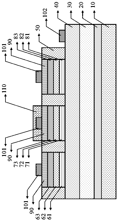
[0049] 1. Production steps:

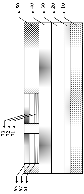
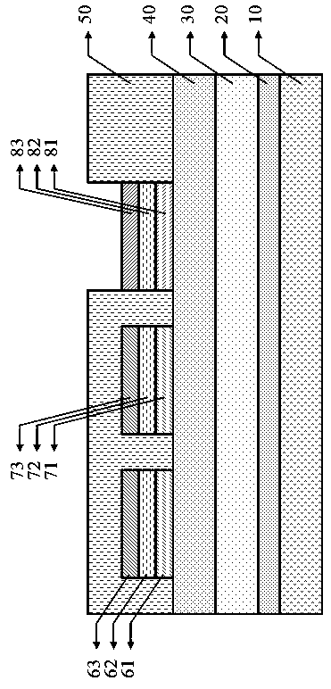
[0050] 1. A substrate 10 is provided, which may be any one of sapphire, silicon, silicon carbide, and gallium nitride, but is not limited thereto.

[0051] 2. In the MOCVD machine, the buffer layer 20 , the unintentionally doped GaN layer 30 and the n-type doped GaN layer 40 are epitaxially grown on the substrate 10 in sequence by using the conventional LED epitaxial growth technology.

[0052] 3. Deposit the insulating dielectric mask layer 50 on the n-type doped GaN layer 40 for the first time by means of plasma enhanced chemical vapor deposition, and then fabricate the first blue photoelectric sensor on the surface of the insulating dielectric mask layer 50 by photolithography. The light-emitting structure layer and the second blue light-emitting light-emitting structure layer area mask, the width of the mask area is between 1 and 100 μm, and the first blue light-emitting structure layer is etched laterally and at intervals by chemical etching ...


PUM


Abstract

The invention provides an integrated light-emitting Micro LED chip and a manufacturing method thereof, which belong to the field of semiconductor optoelectronic technologies. A buffer layer, an unintentionally doped GaN layer and an n-type doped GaN layer epitaxially grow on the same side of a substrate. First and second blue light electroluminescence structure layers and a green light electroluminescence structure layer are etched laterally at intervals by depositing an insulating dielectric mask layer twice, and corresponding light-emitting structure layers are manufactured in correspondingly formed etching areas. Blue light emitted by the second blue light electroluminescence structure layer is converted into red light by a red light photoluminescence conversion layer. According to theinvention, GaN-based blue and green electroluminescence and red light photoluminescence technologies are integrated to produce red, green and blue three-primary-colour MicroLED LED light-emitting units; red, green and blue three-primary-colour light-emitting units are laterally deposited on the n-type doped GaN layer at intervals and are connected through the n-type doped GaN layer.

Description

technical field [0001] The invention belongs to the field of semiconductor photoelectric technology, in particular to the production technology of integrated light-emitting Micro LED chips. Background technique [0002] As a next-generation display technology, Micro LED has broad market prospects and has received widespread attention in the industry. Since Micro LED full-color display needs to integrate high-density micro-sized red, green, and blue three primary color LED chip arrays on one screen, the batched mass transfer technology of red, green, and blue three primary color LED chips has become a constraint for its development. The main technical bottleneck. If the red, green and blue primary color LED chips can be made into a chip-level integrated light-emitting unit, the efficiency of mass transfer can be improved and the complexity of terminal product production can be reduced. [0003] On the other hand, the current red, green, and blue primary color LED chips, gen...

Claims


Application Information

Patent Timeline
Patent Type & Authority Applications(China)
IPC IPC(8): H01L27/15H01L33/00
CPCH01L27/156H01L33/0075
Inventor 李志聪王国宏戴俊吴杰
Owner YANGZHOU ZHONGKE SEMICON LIGHTING
Why Eureka
Try Eureka