Chip scale image sensor and method for fabricating the same

Inactive Publication Date: 2005-11-17
CROSSTEK CAPITAL
View PDF8 Cites 17 Cited by
  • Summary
  • Abstract
  • Description
  • Claims
  • Application Information

AI Technical Summary

Benefits of technology

[0008] Accordingly, the present invention has been made to solve the above-mentioned problems occurring in the prior art, and an object of the

Problems solved by technology

Also, since vapor-disposition, etching and lithography steps are repeated during its fabricating process, the conventional CMOS image sensor has a problem in that there exist defects interrupting light transmission between the micro lens 20 and the photodiode 12 and thus defect pixe

Method used


Image

  • Chip scale image sensor and method for fabricating the same
  • Chip scale image sensor and method for fabricating the same
  • Chip scale image sensor and method for fabricating the same

Examples


Embodiment Construction

[0019] Hereinafter, preferred embodiments of the present invention will be described with reference to the accompanying drawings. In the following description and drawings, the same reference numerals are used to designate the same or similar components, and so repetition of the description on the same or similar components will be omitted.

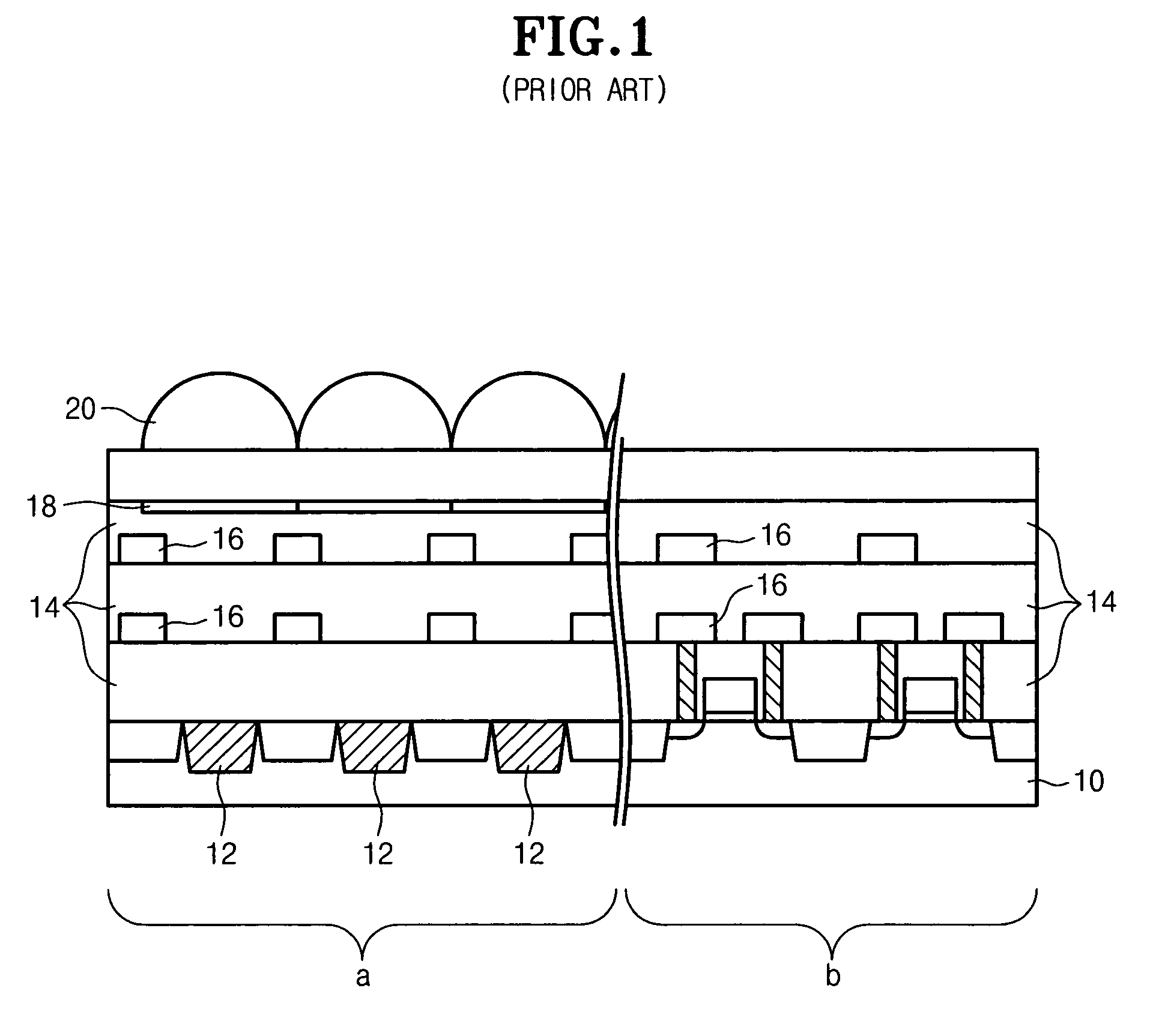
[0020] In an image sensor according to the present invention, a pixel array and a peripheral circuit are separately formed on different substrates and then are connected to each other.

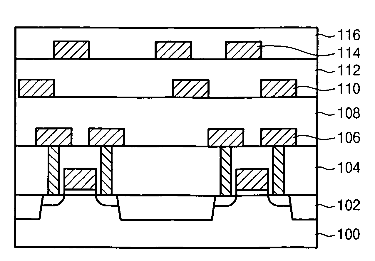
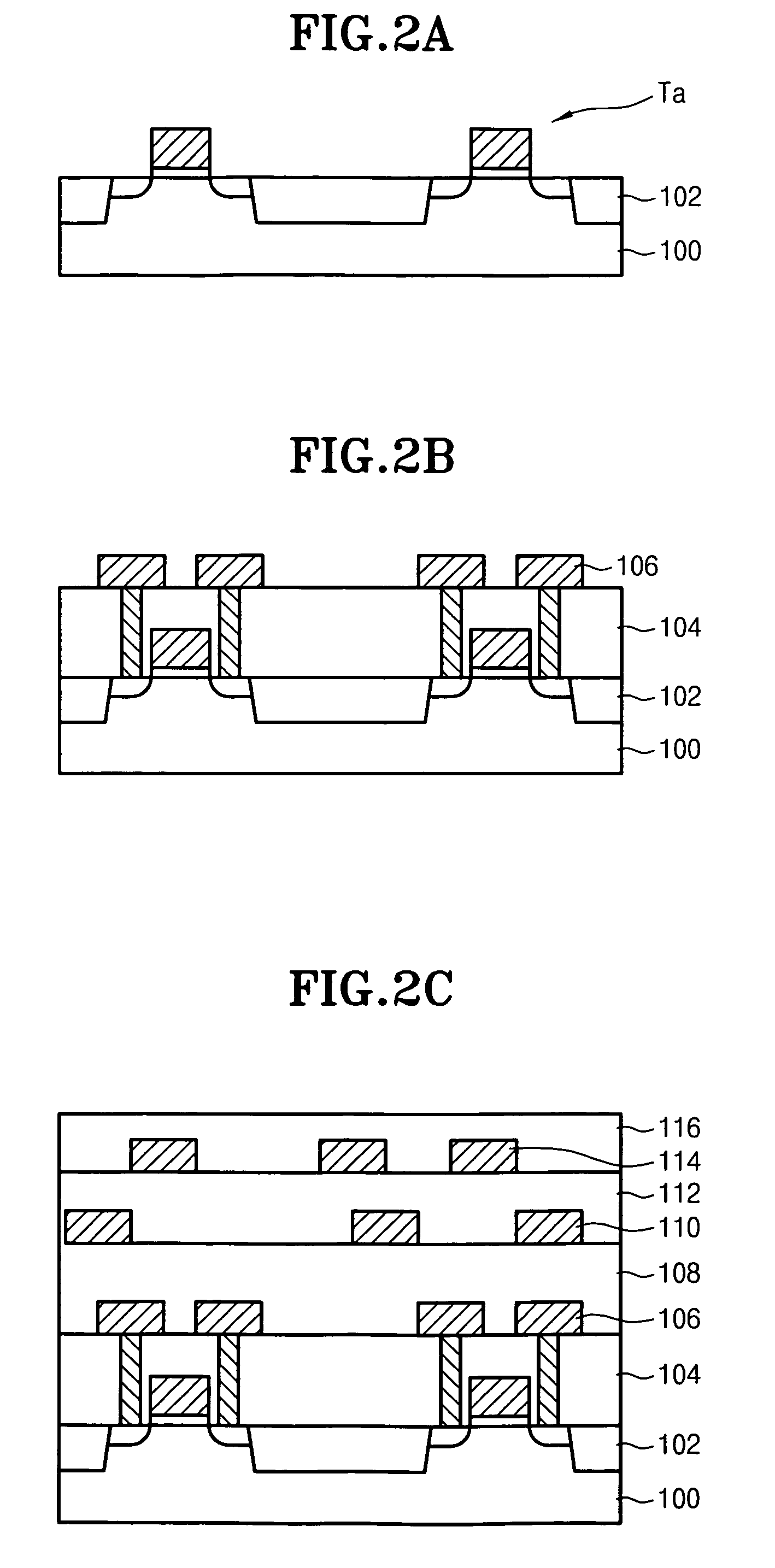
[0021]FIGS. 2a to 2c illustrate process-by-process sectional views showing a method for fabricating the peripheral circuit of the image sensor.

[0022] Referring to FIG. 2a, a device separating film 102 is formed on a first substrate 100 to define an active region, and a transistor Ta is formed the defined active region. Although not shown, various kinds of active and passive devices other than the transistor, such as a diode, a resistor, a capacitor and an inductor...


PUM


Abstract

Disclosed are a chip scale image sensor and its fabricating method. Such a chip scale image sensor includes a first substrate on which a peripheral circuit is formed, a second substrate which is stacked on the first substrate and on which a pixel array is formed, and global interconnections for electrically connecting the pixel array and the peripheral circuit. That is, since a pixel array and a peripheral circuit are separately formed and then are coupled to each other, there is no need to apply a repetitive fabricating process of forming multilayer metal interconnections to the pixel array. Thus, photosensitivity of the pixel array is not lowered, distances between a photodiode, a color filter and a micro lens can be minimized, and sensitivity of the image sensor can be still more improved due to a wide choice of light transmissive films.

Description

BACKGROUND OF THE INVENTION [0001] 1. Field of the invention [0002] The present invention relates generally to an image sensor, and more particularly to an image sensor having a three-dimensional stacked structure and its fabricating method. [0003] 2. Description of the Prior Art [0004] A CMOS image sensor has many advantages over the existing CCD image sensor. For example, its driving scheme is easier than that of the existing CCD image sensor, it can integrate a signal processing circuit on one chip and thus it possible to miniaturize a module of the image sensor, its cost of production can be lowered because an ordinary CMOS fabricating process can be applied to its formation, an so forth. A fabricating process of the CMOS image sensor is similar to that of a semiconductor device. [0005] As shown in FIG. 1, a conventional CMOS image sensor may consist of a pixel region a to which an image is inputted and a peripheral circuit region b around the pixel region a, in which a signal p...

Claims


Application Information

Patent Timeline
IPC IPC(8): H01L23/00H01L27/146H01L31/062
CPCH01L27/14603H01L27/14609H01L27/14621H01L27/14627H01L27/1469H01L27/14645H01L27/14685H01L27/14689H01L27/14634A47F7/146A47F5/02
Inventor PYO, SUNG GYU
Owner CROSSTEK CAPITAL
Why Eureka
Try Eureka