Light-emitting device and display device

a technology of light-emitting devices and display devices, which is applied in the direction of discharge tubes/lamp details, discharge tubes luminescnet screens, electric discharge lamps, etc., can solve the problems of inability to increase the output luminance, and low dielectric strength of the dielectric layer, so as to reduce the cost, increase the luminance, and the effect of high luminan

Inactive Publication Date: 2005-11-17
PANASONIC CORP
View PDF7 Cites 9 Cited by
  • Summary
  • Abstract
  • Description
  • Claims
  • Application Information

AI Technical Summary

Benefits of technology

[0012] The present invention is directed to solving these problems of the prior art, and an object of this invention is to provide an EL device whereby both reduced cost and increased luminance can be simultaneously achieved. A further object is to provide a display device using this EL device.
[0013] An EL device according to the present invention has an emitting layer including a phosphor layer and a dielectric layer, and a pair of electrodes for applying an electric field to the phosphor layer. The dielectric layer is composed of a crystalline material having a perovskite structure in which a lattice constant of a c-axis is greater than a lattice constant of an a-axis. This simultaneously affords high luminance and a low device cost.
[0014] A display device according to the present invention is a passive matrix display device having a light-emitting device composed of striped first electrodes, a dielectric layer, a phosphor layer, and striped second electrodes orthogonal to the first electrodes, and a drive circuit for applying a drive voltage between the first and second electrodes and thereby causing the phosphor layer to emit. The dielectric layer of this light-emitting device is made from a dielectric composed of a crystalline material with a perovskite structure where the lattice constant of the c-axis is greater than the lattice constant of the a-axis obtained by x-ray diffraction. This simultaneously affords high luminance and a low device cost.
[0015] Thus comprised, an EL device and display device according to the present invention afford high luminance because of the high insulation breakdown voltage of the dielectric layer, and reduced cost because a low cost general purpose glass substrate can be used. Our invention thus affords the high luminance and low unit cost that are well suited to televisions and other displays.

Problems solved by technology

As taught in Japanese Patent Laid-open Publication No. 2001-196184, however, due to the low-density of the dielectric crystals formed by thin film deposition, the dielectric strength of the dielectric layer is low.
As a result, when a high voltage is applied to the phosphor layer, the dielectric layer fails, and the output luminance cannot be increased.
A problem with the conventional EL element taught in Japanese Patent Laid-open Publication No. 2001-196184 is that because the dielectric layer is annealed at 1100° C., a special substrate with high heat resistance must be used, and the cost of materials thus rises.
This increases the number of production steps and thus increases production cost.

Method used


Image

  • Light-emitting device and display device
  • Light-emitting device and display device
  • Light-emitting device and display device

Examples


embodiment 1

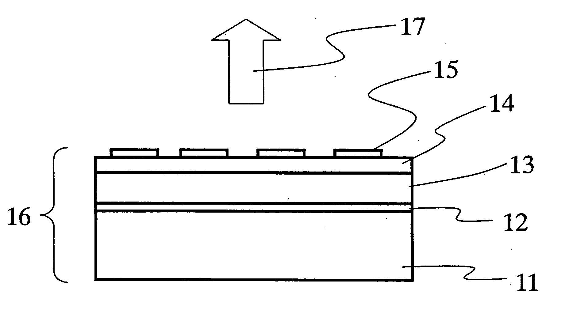
[0033]FIG. 1 is a section view of an EL device according to a first embodiment of the present invention. Sequentially layered on a base substrate 11, this EL device 16 has back electrodes 12 that are the first electrodes in a striped pattern, a dielectric layer 13 formed by thin film deposition of a dielectric material, an phosphor layer 14 made from an inorganic phosphor, and transparent front electrodes 15 that are the second electrodes in a striped pattern. The back electrodes 12 and front electrodes 15 are striped in mutually perpendicular directions. When a voltage is applied between the back electrodes 12 and front electrodes 15, light 17 emitted from the back electrodes 12 at the intersecting portion of the selected back electrodes 12 and the selected front electrodes 15 is emitted passing through the front electrodes 15.

[0034] The components of this EL device 16 are further described below.

[0035] The substrate 11 could be a ceramic substrate, a plastic substrate subjected ...

embodiment 2

[0085]FIG. 10 is a section view of an EL device 102 according to a second embodiment of the present invention. This EL device 102 differs from the EL device in the first embodiment only in having a buffer layer 101 rendered between the back electrodes 12 and dielectric layer 13. Note that like parts here and in FIG. 1 are identified by like reference numerals.

[0086] The composition of the buffer layer 101 is described by the chemical formula MgxSi1-xO (where 0.913 over a buffer layer 101 of this composition affords good crystal characteristics and crystal orientation characteristics in the dielectric. Compositions outside the ranges of this chemical formula disturb the crystal structure of the NaCl structure or the face-centered cubic structure (fcc structure) that is the basic structure of MgO, thus degrade the crystal orientation, and are therefore undesirable.

[0087] Table 3 shows the results of tests exploring the relationship between the film thickness of the buffer layer 101 ...

embodiment 3

[0088]FIG. 11 is a section view of an EL device 112 according to a third embodiment of the present invention. Compared with the EL devices of the first and second embodiments, this EL device 112 is the same as the EL devices shown in FIG. 1 and FIG. 10 except that a bottom layer 111 is rendered between the substrate 11 and the back electrodes 12 made of a conductor containing one of Pt, Pd, Au, Ir, Rh, and Ni.

[0089] The bottom layer 111 is a 5 nm to 50 nm thick film of Ti, Co, or Ni. Rendering this bottom layer 111 improves adhesion between the substrate 11 and back electrodes 12.


PUM


Abstract

A light-emitting device having first electrodes, a dielectric layer, a phosphor layer, and second electrodes layered sequentially on a substrate, the dielectric layer is made from a dielectric composed of a crystalline material with a perovskite structure where the lattice constant of the c-axis is greater than the lattice constant of the a-axis obtained by x-ray diffraction.

Description

BACKGROUND OF THE INVENTION [0001] 1. Field of Technology [0002] The present invention relates to a light-emitting device that emits light when voltage is applied to an inorganic phosphor, and to a display device using this light-emitting device. [0003] 2. Description of Related Art [0004] Light-emitting devices (electroluminescent devices, referred to as “EL devices” below) that use an inorganic phosphor such as zinc sulfide as the luminous element are self-emissive and feature excellent readability, a wide viewing angle, and fast response. Due to these characteristics, EL elements are well-suited for application in television displays, personal computer displays, and other types of display devices. As a result, various proposals have been made to provide practical low cost, high luminance EL devices. [0005] A typical EL device has a first electrode layer, an emitting layer including a dielectric layer and an inorganic phosphor layer, and a second electrode layer built over a base ...

Claims


Application Information

Patent Timeline
Patent Type & Authority Applications(United States)
IPC IPC(8): H01J1/62H01L21/316H05B33/22
CPCH05B33/22H01L21/31691H01L21/02197
Inventor NASU, SHOGOONO, MASAYUKIAOYAMA, TOSHIYUKIODAGIRI, MASARU
Owner PANASONIC CORP
Why Eureka
Try Eureka