Silicon carbide semiconductor device and method for manufacturing the same

Inactive Publication Date: 2005-11-24
DENSO CORP +1
View PDF8 Cites 54 Cited by
  • Summary
  • Abstract
  • Description
  • Claims
  • Application Information

AI Technical Summary

Benefits of technology

[0017] In the above method provides the silicon carbide semiconductor device having the gate layer thicker than that of a conventional device. Accordingly, input resistance of the gate becomes lower. Further, the gate layer on the inner wall of the first trench is formed by the epitaxial method so that the shape of the gate layer is traced along with the shape of the inner wall of the first trench. Thus, the gate layer has no step portion so that electric field concentration at the corner of the gate layer is suppressed. Therefore, the withstand voltage between the gate and the drain in the device becomes higher. Accordingly, the method provides the silicon carbide semiconductor device having excellent electric properties.
[0027] The above device provides a JFET including the substrate as a drain, the first semiconductor layer as a source and a part of the drift layer as a channel. The guard ring has the depth equal to the depth of the gate layer in the cell portion. Accordingly, input resistance of the gate becomes lower. Further, the withstand voltage between the gate and the drain in the device becomes higher. Thus, the method provides the silicon carbide semiconductor device having excellent electric properties.

Problems solved by technology

However, the above-described conventional silicon carbide semiconductor device owns the below-mentioned problems.
As a first problem, an input resistance of the gate is high.
However, in this ion implantation method, ion implanting apparatus with high energy is required.
Also, when the ions are implanted in the high energy, damages may remain when the ions are implanted, and there is a risk that a junction between a gate and a drain may be destroyed.
Therefore, this ion implantation method with the high energy is not preferably acceptable.
As a second problem, a withstanding voltage between the gate and the drain is low.
As a third problem, a contact resistance between a gate layer and a gate electrode is high.
In such a structure, even when an input resistance of a gate is tried to be lowered in order to increase a switching speed, in the case that a cell size is, for instance, 3 μm, or 4 μm, the input resistance of the gate could not be sufficiently lowered.
As a fourth problem, in such a case that while a motor, or the like is connected to the silicon carbide semiconductor device, this silicon carbide semiconductor device is operated, there is a risk that a gate driving circuit is destroyed.

Method used


Image

  • Silicon carbide semiconductor device and method for manufacturing the same
  • Silicon carbide semiconductor device and method for manufacturing the same
  • Silicon carbide semiconductor device and method for manufacturing the same

Examples


first embodiment

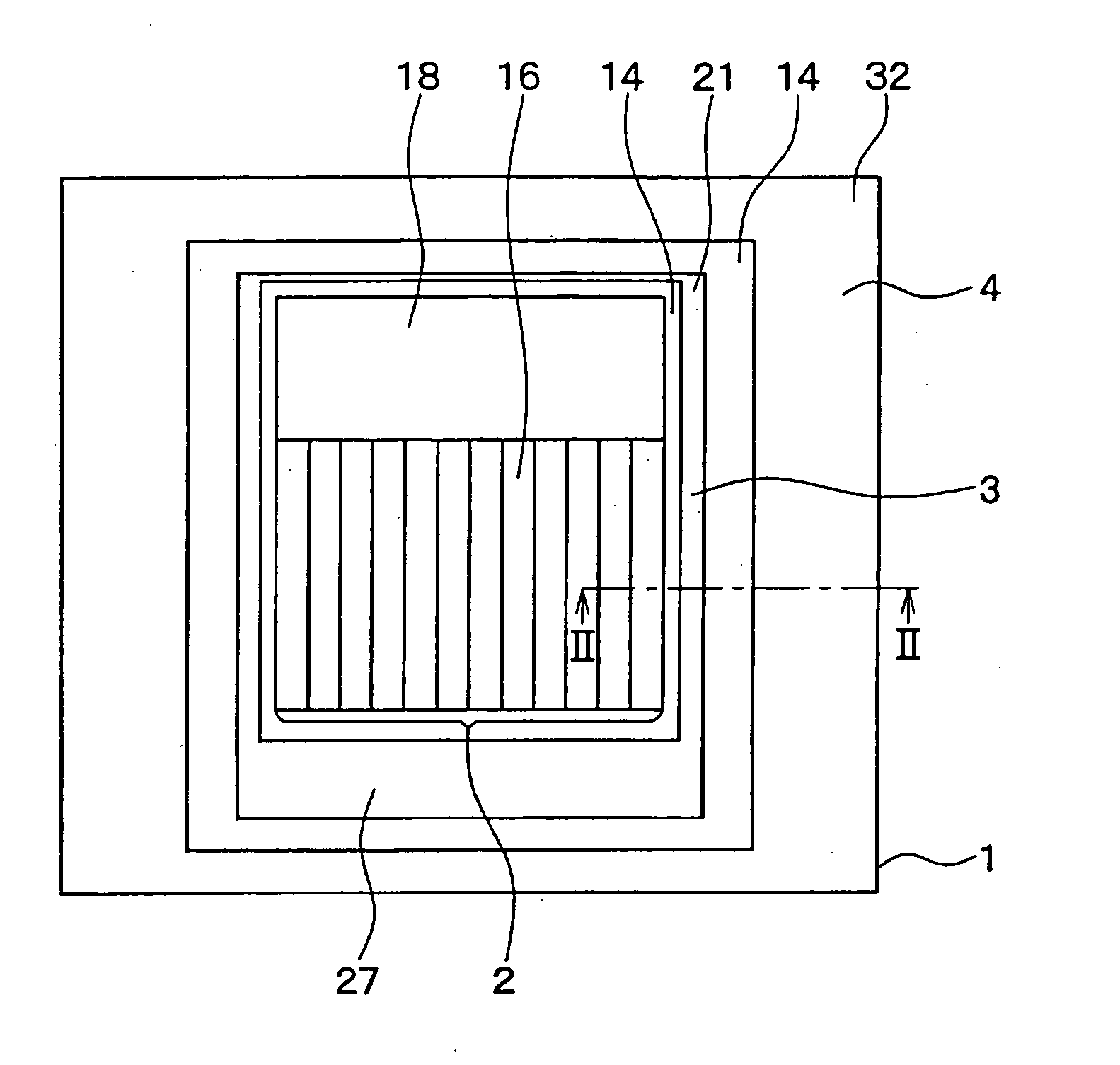
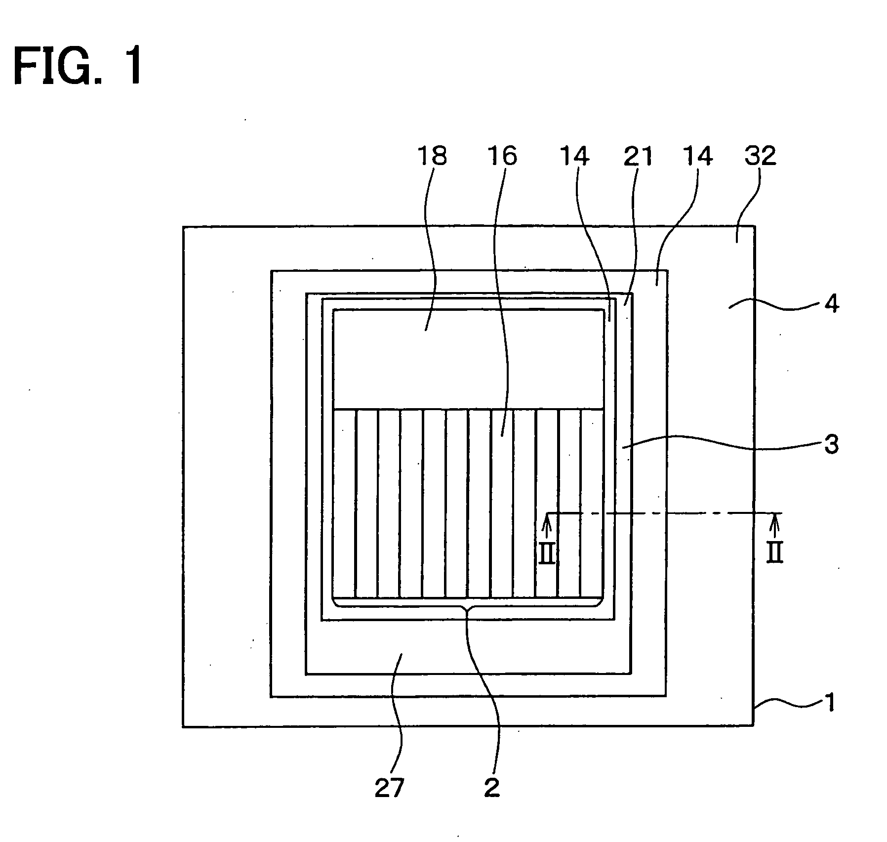
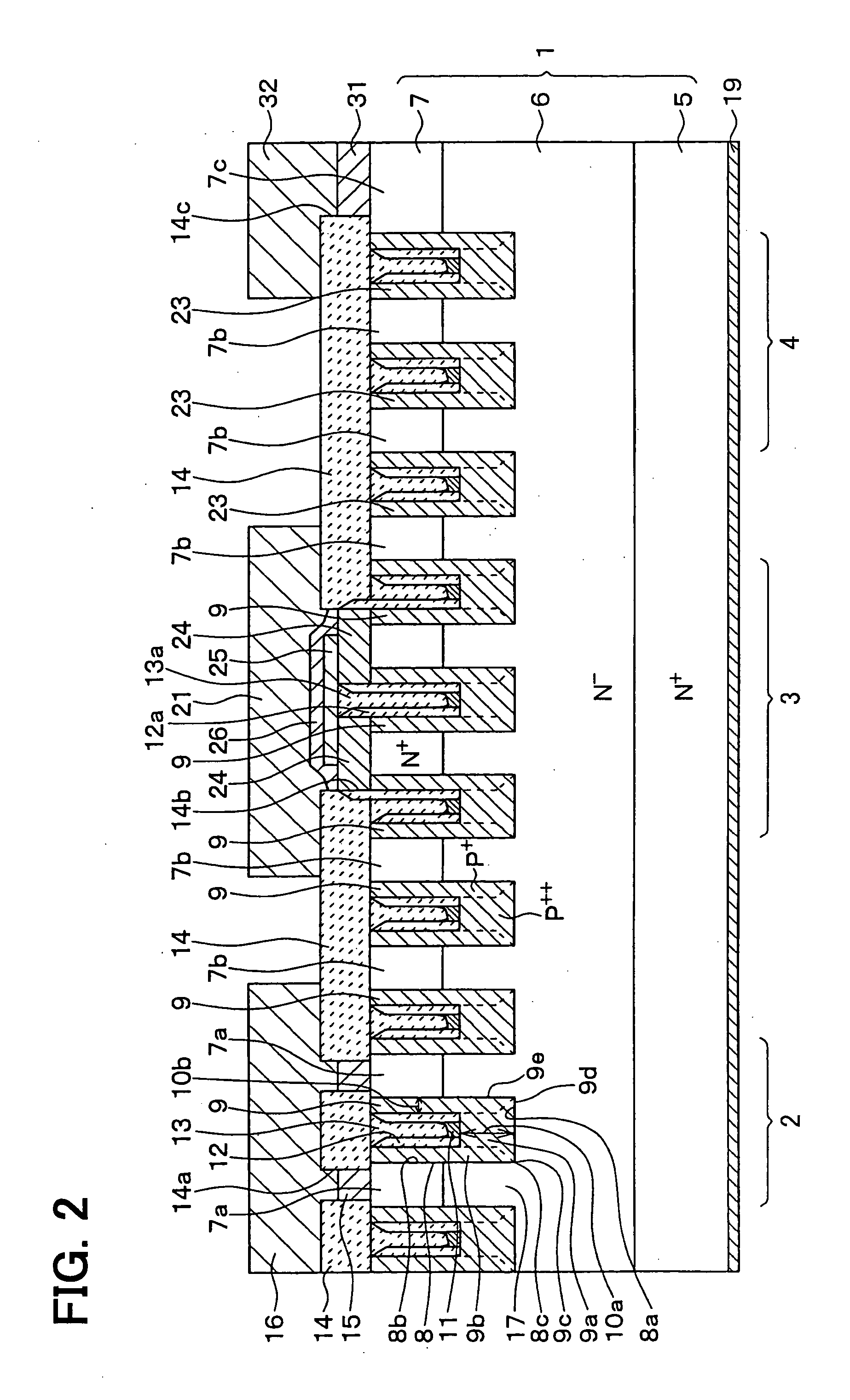
[0061]FIG. 1 is a plan view for showing a silicon carbide semiconductor device equipped with a JFET, according to a first embodiment mode of the present invention. Also, FIG. 2 is a cross sectional view for indicating the semiconductor device, taken along a line II-II shown in FIG. 1.

[0062] As represented in FIG. 1 and FIG. 2, the silicon carbide semiconductor device of this first embodiment mode has been equipped with a cell portion 2, a gate wiring portion 3, and an outer peripheral portion 4. The cell portion 2 is located at a center of a semiconductor substrate 1. The gate wiring portion 3 and the outer peripheral portion 4 are sequentially positioned on the outer peripheral side of this cell portion 2.

[0063] As illustrated in FIG. 2, in the semiconductor substrate 1, an N− type drift layer 6 and an N+ type semiconductor layer 7 functioning as a first semiconductor layer have been sequentially formed on a major surface of an N+ type substrate 5. In this first embodiment mode, ...

second embodiment

[0120]FIG. 17 is a plan view for indicating a silicon carbide semiconductor device according to a second embodiment mode of the present invention. FIG. 18 is a cross sectional view for showing the silicon carbide semiconductor device, taken along a line XVIII-XVIII of FIG. 17.

[0121] A major different point of the semiconductor device according to this second embodiment mode from the semiconductor device of the first embodiment mode is given as follows: That is, as represent in FIG. 17 and FIG. 18, both a body diode portion 51 and a floating P type layer region 52 are provided between the cell portion 2 and the outer peripheral portion 4 with respect to the semiconductor device according to the first embodiment mode.

[0122] In this second embodiment mode, as shown in FIG. 17, the body diode portion 51 has been arranged between the cell portion 2 and the gate wiring portion 3. Precisely speaking, two sets of the body diode portions 51 have been arranged in a region 651a which is diff...

third embodiment

[0157]FIG. 19 is a sectional view for indicating a silicon carbide semiconductor device according to a third embodiment mode of the present invention. In the first and second embodiment modes, the description has been made of such a case that the P type gate layer 9 having the U-shaped form has been formed in the cell portion 2. Alternatively, P type gate layers 9 can be formed by completely embedding P type semiconductor layers inside trenches 8. In other words, the shapes of the P type gate layers 9 can be alternatively made in such same shapes as the portions which have been removed by forming the trenches 8 in the semiconductor substrate 1 when the trenches 8 are formed in the semiconductor substrate 1.

[0158] Next, a method for manufacturing this silicon carbide semiconductor device will now be described. The manufacturing steps of the first embodiment mode are modified as follows: That is, in the step shown in FIG. 5, a P type semiconductor layer 41 formed on the surface of th...


PUM


Abstract

A manufacturing method of a silicon carbide semiconductor device includes the steps of: preparing a semiconductor substrate including a silicon carbide substrate, a drift layer and a first semiconductor layer; forming a plurality of first trenches in a cell portion; forming a gate layer on an inner wall of each first trench by an epitaxial growth method; forming a first insulation film on the surface of the semiconductor substrate; forming a gate electrode on the first insulation film for connecting to the gate layer electrically; forming a source electrode on the first insulation film for connecting to the first semiconductor layer in the cell portion; and forming a drain electrode connected to the silicon carbide substrate electrically.

Description

CROSS REFERENCE TO RELATED APPLICATIONS [0001] This application is based on Japanese Patent Applications No. 2004-153126 filed on May 24, 2004, and No. 2004-153127 filed on May 24, 2004, the disclosures of which are incorporated herein by reference. FIELD OF THE INVENTION [0002] The present invention relates to a silicon carbide semiconductor device and a method for manufacturing the device. BACKGROUND OF THE INVENTION [0003] A silicon semiconductor device equipped with a guard ring in a peripheral portion of a semiconductor chip is well-known. FIG. 31 shows a cross sectional view of this silicon semiconductor device. This semiconductor device is provided with a semiconductor substrate 103 having an N− type epitaxial layer 102 formed on an N+ type silicon semiconductor substrate 101. In a cell portion of this semiconductor device, a P type body region 106 has been formed on a surface layer of the epitaxial layer 102, and an N+ type source region 105 has been formed within the P type...

Claims


Application Information

Patent Timeline
IPC IPC(8): H01L21/04H01L21/336H01L27/098H01L27/10H01L29/06H01L29/24H01L29/78H01L29/808
CPCH01L27/098H01L29/0619H01L29/8083H01L29/66068H01L29/1608
Inventor KUMAR, RAJESHYAMAMOTO, TSUYOSHINAKAMURA, HIROKIMORISHITA, TOSHIYUKIOHYANAGI, TAKASUMIWATANABE, ATSUO
Owner DENSO CORP
Why Eureka
Try Eureka