Manufacturing method of a semiconductor device

Inactive Publication Date: 2005-11-24
RENESAS TECH CORP
View PDF2 Cites 60 Cited by
  • Summary
  • Abstract
  • Description
  • Claims
  • Application Information

AI Technical Summary

Benefits of technology

[0008] In the semiconductor device manufacturing process, there is a tendency to increase the diameter of a semiconductor wafer in order to increase the number of semiconductor chips that are capable of being obtained from a single semiconductor wafer, thereby to improve the production yield of semiconductor devices. But, the above-described problem becomes more and more conspicuous with an increase in the diameter of the semiconductor wafer.
[0012] It is an object of the present invention to provide a technique which is capable of improving the reliability of a thin semiconductor device.
[0013] It is another object of the present invention to provide a technique which is capable of improving the yield of a thin semiconductor wafer.
[0018] After the back surface of the semiconductor wafer is subjected to grinding and polishing in a state in which a tape having a frame portion is affixed to the wafer main surface, the semiconductor wafer with the tape affixed thereto is cut into individual semiconductor chips, whereby it is possible to suppress or prevent quality deterioration of the thin semiconductor wafer or semiconductor chips in the back-end process, and, hence, it is possible to improve the reliability of a thin semiconductor device.
[0019] Further, by conveying the semiconductor wafer in a state in which a tape having a frame portion is affixed to the wafer main surface, it is possible to suppress or prevent cracking of the semiconductor wafer, and, hence, it is possible to improve the production yield of a thin semiconductor device.

Problems solved by technology

However, the present inventors have found that an attempt to meet such a demand for the thinning of semiconductor chips encounters the following problems in the back-end process during manufacture of the semiconductor device.
However, the tape affixed to the main surface of the semiconductor wafer cannot be very thick from the standpoint of ensuring easiness of subsequent peeling of the tape.
Therefore, as the semiconductor wafer becomes thinner, it is impossible, with only the tape affixed to the wafer main surface, to fully support the semiconductor wafer after the back grinding and polishing steps.
Consequently, it becomes difficult to transfer the semiconductor wafer to the subsequent step in the manufacture.
In more particular terms, since the tape has a lower rigidity than the semiconductor wafer, the semiconductor wafer, after the back grinding and polishing steps, warps while following the shape of the affixed tape, thus giving rise to the problem that the semiconductor wafer may crack during its transfer.
But, the above-described problem becomes more and more conspicuous with an increase in the diameter of the semiconductor wafer.
Consequently, there arises a problem in that, if the accuracy of the tape thickness varies, the accuracy of the wafer thickness also varies.
Particularly, as the semiconductor wafer becomes thinner, the relative thickness of the tape affixed to the main surface of the semiconductor wafer increases, so that variations in the tape thickness accuracy come to be further actualized, thus leading to the problem that the semiconductor wafer grinding accuracy and polishing accuracy are deteriorated.

Method used


Image

  • Manufacturing method of a semiconductor device
  • Manufacturing method of a semiconductor device
  • Manufacturing method of a semiconductor device

Examples


first embodiment

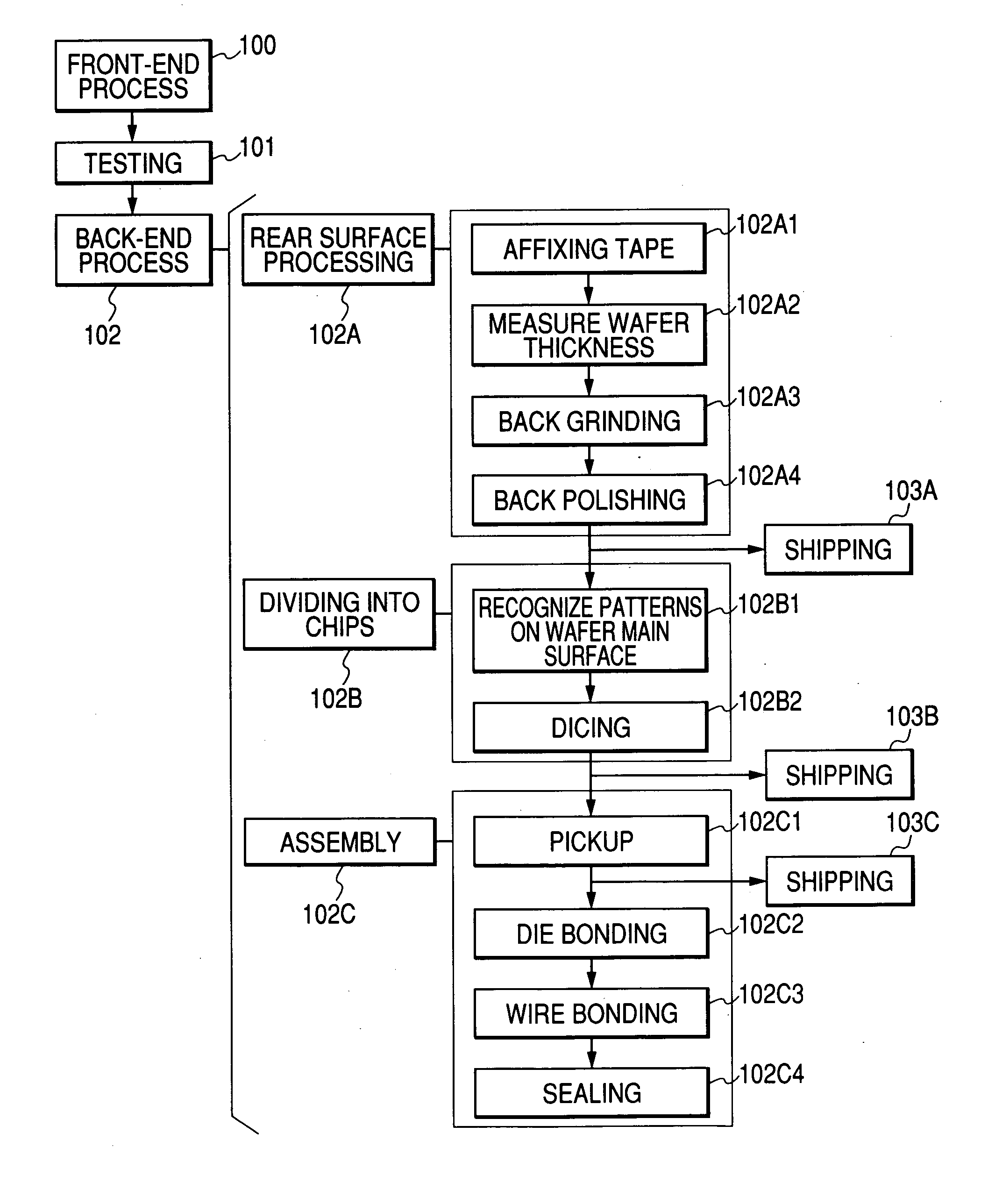
[0068] A semiconductor device manufacturing process according to a first embodiment of the present invention will be described below on the basis of the flow chart of FIG. 1 and with reference to FIGS. 2 to 28.

[0069] First, in a front-end process 100, a semiconductor wafer (hereinafter referred to simply as a “wafer”) having a substantially circular plane shape and a diameter of 300 mm or so, for example, is provided, and plural semiconductor chips (simply “chips” hereinafter) are formed on a main surface of the wafer. The front-end process 100 is also called a wafer process, diffusion process, or wafer fabrication, in which chips (elements and circuits) are formed on the main surface of the wafer and preparations are made so as to permit electric tests to be performed using probes or the like. The front-end process comprises a film forming process, an impurity introducing (diffusion or ion implantation) process, a photolithography process, an etching process, a metallizing process...

second embodiment

[0094] In connection with this second embodiment, a description will be given concerning a conveyance tray for thin chips. FIG. 30 is a sectional view of a principal portion of an ordinary type of conveyance tray 90. With a decrease in thickness of chips 1C, pockets 90a formed in the conveyance tray 90 are also becoming shallower, while taking product protectiveness into account. However, if the pockets 90a are too shallow, when a chip 1C is accommodated into or removed from a pocket 90a, this chip accommodating or removing work affects other chips 1C already received in adjacent pockets 90a, thus giving rise to the problem that the other chips 1C move out of the pockets 90a. FIG. 31 shows an example of this state, in which a chip 1C is about to be received in a pocket 90a. Usually, for accommodating a chip 1C into a pocket 90a formed in the conveyance tray 90, the chip 1C is vacuum-chucked by the collet (an inverted pyramidal collet is illustrated) and, in this state, is conveyed t...

third embodiment

[0108] In connection with this third embodiment, a modification of the wafer thickness measuring step 102A2 shown in FIG. 1 will be described. FIG. 43 illustrates a wafer thickness measuring step according to this third embodiment.

[0109] In this third embodiment, the thickness of the wafer 1W is measured using a thickness gauge 30 beforehand in an off-line manner and the data obtained is transferred to the rear surface processing apparatus. In the same apparatus, the back surface height of the wafer 1W placed on the vacuum chuck stage is detected, and the wafer back surface is subjected to grinding and polishing by a required quantity taking the measured value of the wafer thickness into account. According to this third embodiment, it is possible to eliminate the need for use of an expensive IR camera.


PUM


Abstract

The reliability of a thin semiconductor device is to be improved. A tape having a ring affixed to an outer periphery thereof is affixed to a main surface of a semiconductor wafer, and, in this state, a back surface of the semiconductor wafer is subjected to grinding and polishing to thin the wafer. Thereafter, the semiconductor wafer is conveyed to a dicing apparatus in a state in which the tape with the ring is affixed to the wafer main surface without peeling of the tape, and dicing is performed from the back surface side of the semiconductor wafer to divide the wafer into individual semiconductor chips. With this method, handling of the thin semiconductor wafer by rear surface processing can be facilitated. Besides, the manufacturing process can be simplified because the replacement of the tape is not needed at the time of shift from rear surface processing to the dicing process.

Description

CROSS-REFERENCE TO RELATED APPLICATION [0001] The present application claims priority from Japanese patent application No. 2004-150048, filed on May 20, 2004, the content of which is hereby incorporated by reference into this application. BACKGROUND OF THE INVENTION [0002] The present invention relates in general to a semiconductor device manufacturing technique and, more particularly, to a technique which may be used for thinning a semiconductor device. [0003] A conventional back-end process in the manufacture of a semiconductor device is carried out as follows. First, a tape is affixed to a main surface of a semiconductor wafer, and then a back surface of the semiconductor wafer is subjected to grinding and then to polishing. Subsequently, the tape is peeled from the main surface of the semiconductor wafer, then the back surface of the semiconductor wafer is affixed to a dicing tape, and, thereafter, a dicing blade is positioned in a cutting region on the main surface of the semic...

Claims


Application Information

Patent Timeline
IPC IPC(8): H01L21/304H01L21/301H01L21/46
CPCH01L21/3043H01L21/304H01L21/78
Inventor UEMATSU, TOSHIHIDEMIYAZAKI, CHUICHIABE, YOSHIYUKIKIMURA, MINORU
Owner RENESAS TECH CORP
Why Eureka
Try Eureka