Plasma processing apparatus and plasma processing method

a processing apparatus and plasma technology, applied in the field of plasma processing apparatus and plasma processing method, can solve the problems of abnormal discharge, processing apparatus damage, abrupt abnormal discharge, etc., and achieve the effect of enhancing the reliability and productivity of semiconductor devices

Inactive Publication Date: 2005-12-01
SEMICON TECH ACADEMIC RES CENT
View PDF1 Cites 27 Cited by
  • Summary
  • Abstract
  • Description
  • Claims
  • Application Information

AI Technical Summary

Benefits of technology

[0014] According to the above method, the current induced by the ultraviolet light generated from the plasma is detected by the photon detection sensor mounted on the wafer stage while the plasma processing of the substrate is being performed; in this way, any abnormal discharge occurring in the plasma chamber can be detected in real time in the form of a change in current value. Accordingly, quick action can be taken to deal with the abnormality, offering the effect of enhancing the reliability and productivity of semiconductor devices.

Problems solved by technology

However, one problem involved with such plasma processes is that an abnormal discharge can occur abruptly during processing in a plasma processing apparatus.
In the worst case, the processing-apparatus may be damaged.
An abnormal discharge occurs when the large electric charge accumulated on the inside wall of the plasma chamber, etc. either exceeds a limit or is discharged for some reason during plasma processing.
As such discharge occurs in an unpredictable manner, and as there are no effective sensing methods for detecting the occurrence, with a prior known plasma processing apparatus, it has not been possible to take appropriate action by detecting the occurrence of such an abnormal discharge in real time, and this has led to the degradation of the productivity, as well as the reliability, of the produced semiconductor device.
This system is one that monitors the energy distribution, ion current, etc., for example, of the ions, electrons, and other particles generated by the plasma, but, as these changes manifest themselves relatively slowly on the semiconductor wafer in contrast with an instantaneous change in the plasma state such as an abnormal discharge, the proposed system is not suitable for real-time monitoring of an abnormal discharge.

Method used


Image

  • Plasma processing apparatus and plasma processing method
  • Plasma processing apparatus and plasma processing method
  • Plasma processing apparatus and plasma processing method

Examples


first embodiment

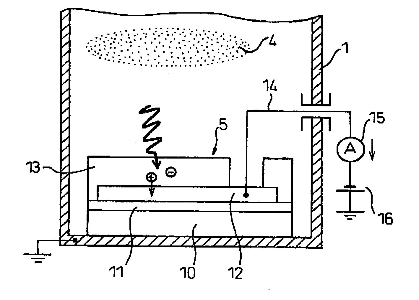
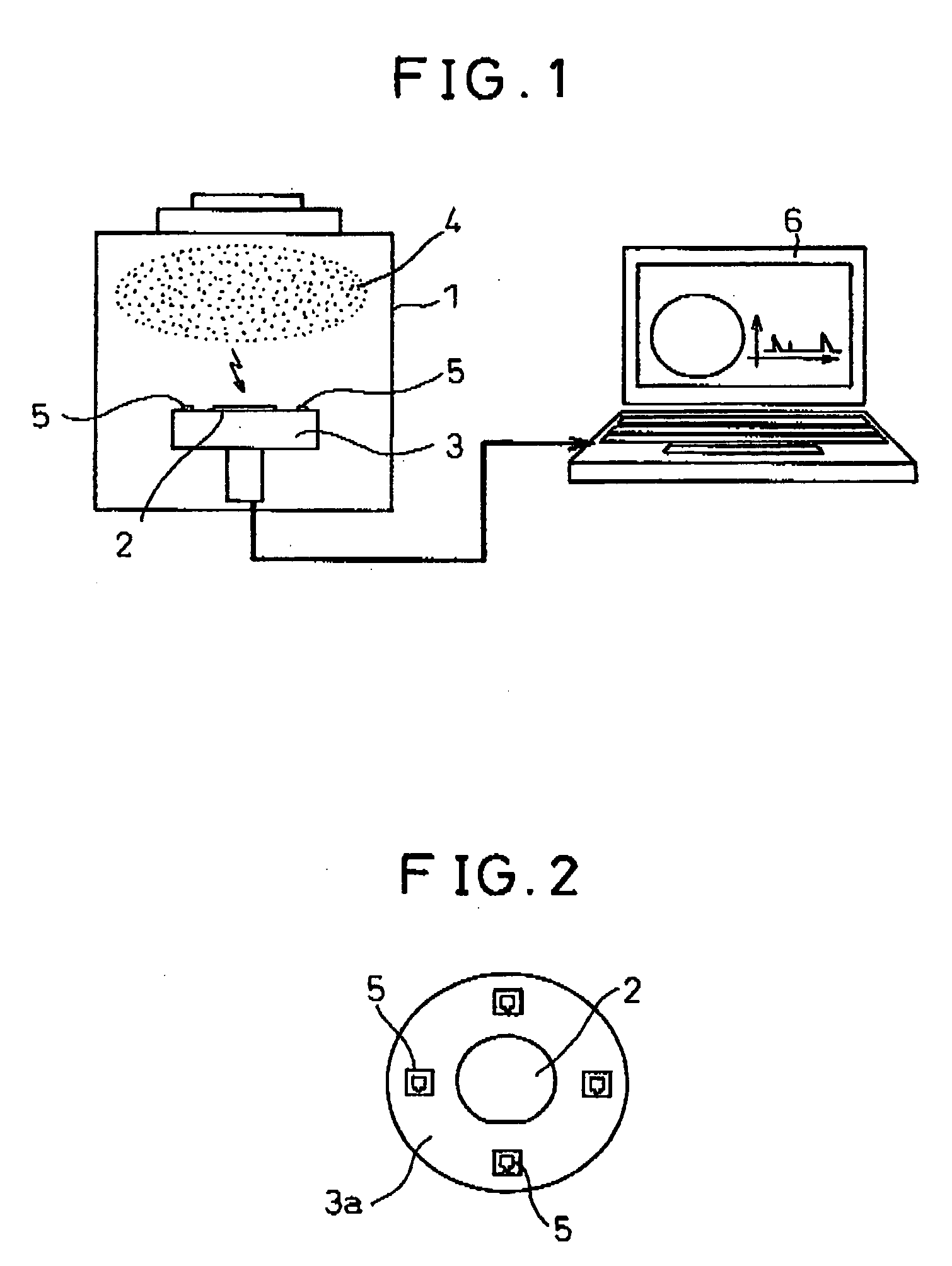
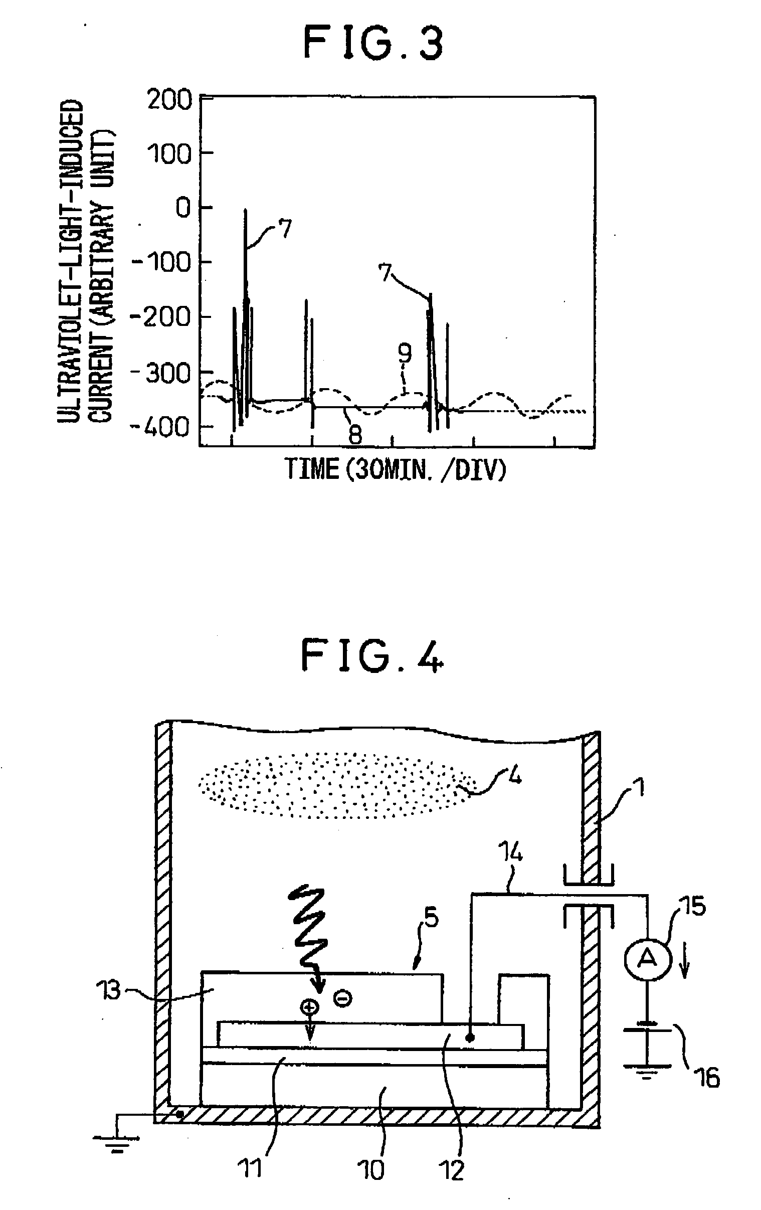
[0032]FIG. 4 shows the photon detection sensor 5. In FIG. 4, for convenience of explanation, the photon detection sensor 5 is shown as being mounted directly on the bottom of the chamber, but in practice, the sensor is mounted on the wafer stage 3 on which the semiconductor wafer is to be held, as shown in FIG. 1. In the figures hereinafter given, the same reference numerals as those in FIGS. 1 and 2 designate the same or similar component elements, and the description of such elements will not be repeated here.

[0033] In the photon detection sensor 5 shown in FIG. 4, reference numeral 10 is a Si semiconductor substrate, 11 is a first insulating film formed from SiO2 or the like, 12 is an electrode formed from Al, and 13 is a second insulating film formed from SiO2 or the like. A portion of the second insulating film 13 is removed by suitable means such as etching to expose a portion of the electrode 12. A wiring line 14 is connected to the exposed portion, and the current flowing in...

second embodiment

[0045]FIG. 7 is a diagram showing the photon detection sensor used in the plasma processing apparatus of the present invention. The photon detection sensor 50 of this embodiment differs from the photon detection sensor 5 of the structure shown in FIG. 4 in that the SiO2 film 13 is covered with an Al film 17 about 100 nm in thickness. Reference numeral 12a indicates the lead terminal of the electrode 12.

[0046] Ions, neutral particles, electrons, and ultraviolet light are generated in the plasma. Therefore, in the photon detection sensor 5 of FIG. 4, the SiO2 film 13 is affected by charged particles such as ions and electrons, causing a variation in the measured current value. In the photon detection sensor 50 shown in FIG. 7, the film 13 is covered with the Al thin film 17 to prevent such particles from penetrating into the film 13. It is known that ultraviolet light with wavelengths of about 17 nm to 90 nm passes through the Al film. Therefore, by depositing the Al film 17 over the ...


PUM

PropertyMeasurementUnit
thicknessaaaaaaaaaa
thicknessaaaaaaaaaa
thicknessaaaaaaaaaa

Abstract

In a plasma processing apparatus which includes a chamber (1) equipped with a wafer stage (3) for mounting thereon a substrate (2) to be processed, and which processes the substrate (2) by exposure to a plasma (4), a photon detection sensor (5) for measuring an ultraviolet-light-induced current is placed on a circumferential portion of a substrate mounting surface (3a) of the wafer stage (3) so that the occurrence of an abnormal discharge can be detected, in real time, from a change in the output of the photon detection sensor (5).

Description

CROSS-REFERENCE TO RELATED APPLICATION [0001] This application claims priority of Japanese Patent Application No. 2004-159531, filed on May 28, 2004. FIELD OF THE INVENTION [0002] The present invention relates to a plasma processing apparatus, and to a plasma processing method, for processing a semiconductor wafer or the like and, more particularly, to a plasma processing apparatus and to a plasma processing method capable of monitoring, in real time, an abnormal discharge phenomenon that can occur during plasma processing. BACKGROUND OF THE INVENTION [0003] Plasma processes such as etching, thin-film deposition, etc. are indispensable for achieving high-quality, high-functionality semiconductor devices. However, one problem involved with such plasma processes is that an abnormal discharge can occur abruptly during processing in a plasma processing apparatus. If an abnormal discharge occurs, etching and thin-film deposition conditions change and, as a result, the characteristics of ...

Claims


Application Information

Patent Timeline
Patent Type & Authority Applications(United States)
IPC IPC(8): H05H1/00C23F1/00G01R31/12H01J37/32H01L21/205H01L21/3065
CPCG01R31/1263H01J2237/0206H01J37/32935
Inventor SAMUKAWA, SEIJINISHIKAWA, SATOSHIKADOMURA, SHINGO
Owner SEMICON TECH ACADEMIC RES CENT
Why Eureka
Try Eureka