Semiconductor device and manufacturing process therefor

a semiconductor and manufacturing process technology, applied in semiconductor devices, semiconductor/solid-state device details, electrical equipment, etc., can solve the problems of reducing the yield of device fabrication and tat, affecting the quality of semiconductor devices, etc., to achieve short tat, high practicability, and high reliability

Inactive Publication Date: 2005-12-01
RENESAS TECH CORP
View PDF3 Cites 235 Cited by
  • Summary
  • Abstract
  • Description
  • Claims
  • Application Information

AI Technical Summary

Benefits of technology

[0023] (3) It is possible to correspond to a process for connection between chips with a method same as the conventional compression bonding method using gold stud bumps. That is, it is possible to realize a unique connection structure having a high reliability by the caulking action using a plastic flow deformation of metallic bumps in a very-low-cost and short-TAT process and provide a three-dimensional inter-chip connection structure having a high practicability.

Problems solved by technology

However, because the difference between reference dimensions of the device fabrication process and the mounting process is two digits or more, forming a through-hole electrode assuming inter-chip connection according to the mounting process simultaneously in the device fabrication process may decrease the yield in device fabrication and TAT.
Moreover, a method for forming a bump electrode at a through-hole portion in a chip through the plating growth disclosed in JP-A-2000-260934 has problems that the plating growth normally requires a lot of time (several hours or more) and it is technically difficult to perform uniform growth including a through-hole portion.

Method used


Image

  • Semiconductor device and manufacturing process therefor
  • Semiconductor device and manufacturing process therefor
  • Semiconductor device and manufacturing process therefor

Examples


embodiment 1

[0054] FIGS. 1 to 14 are illustrations of a semiconductor device of embodiment 1 of the present invention.

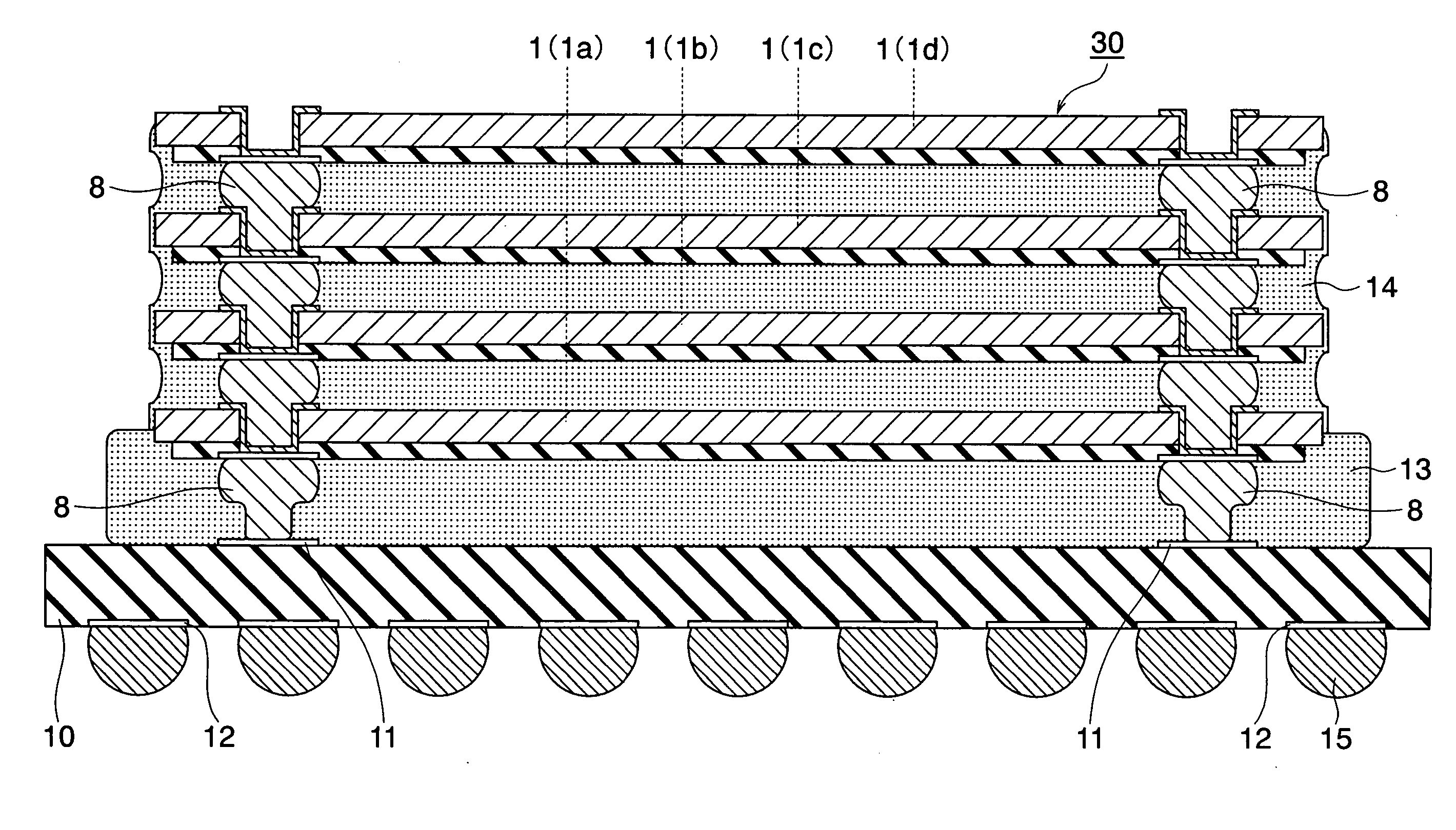
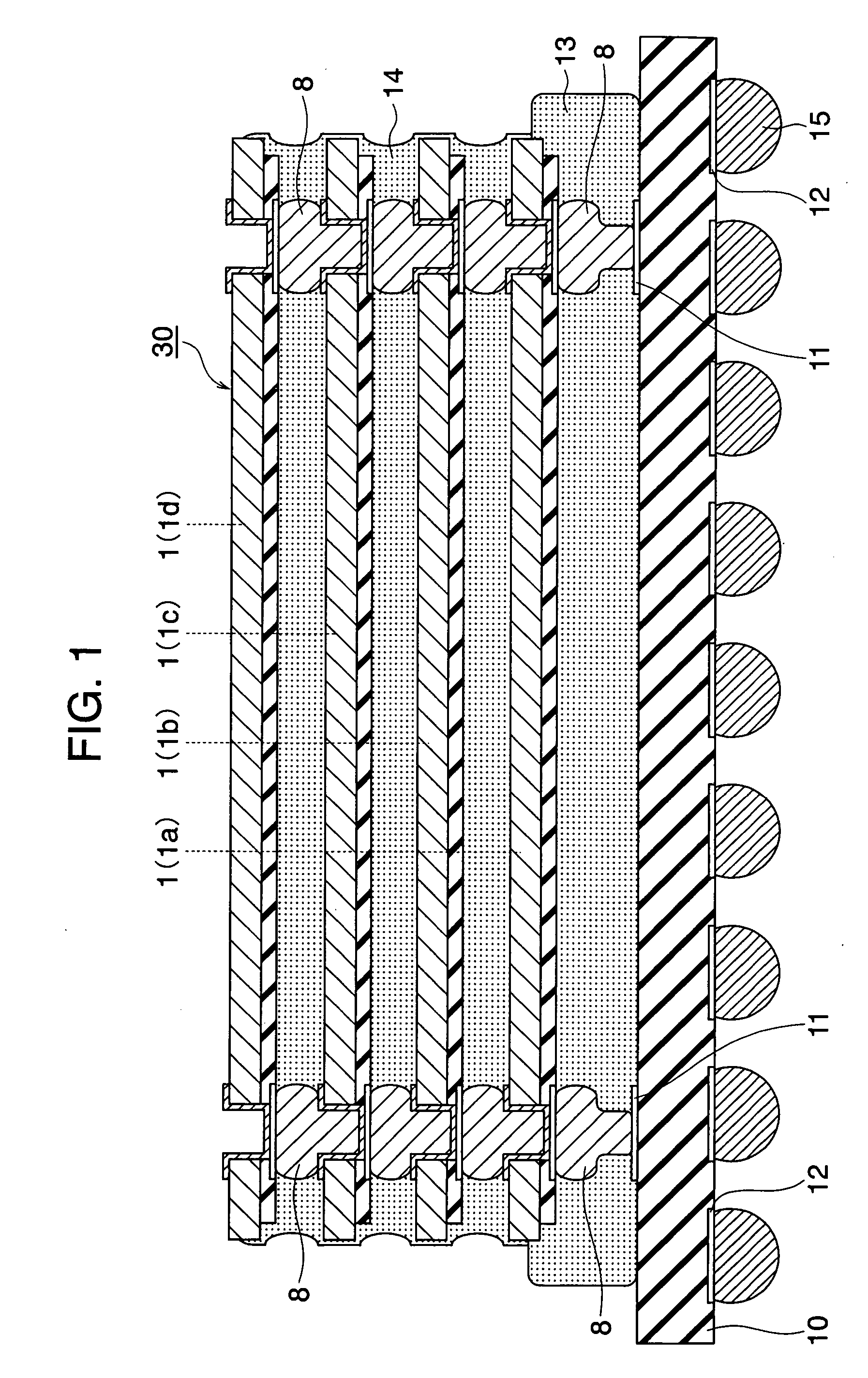
[0055]FIG. 1 is a schematic sectional view showing a schematic configuration of the semiconductor device.

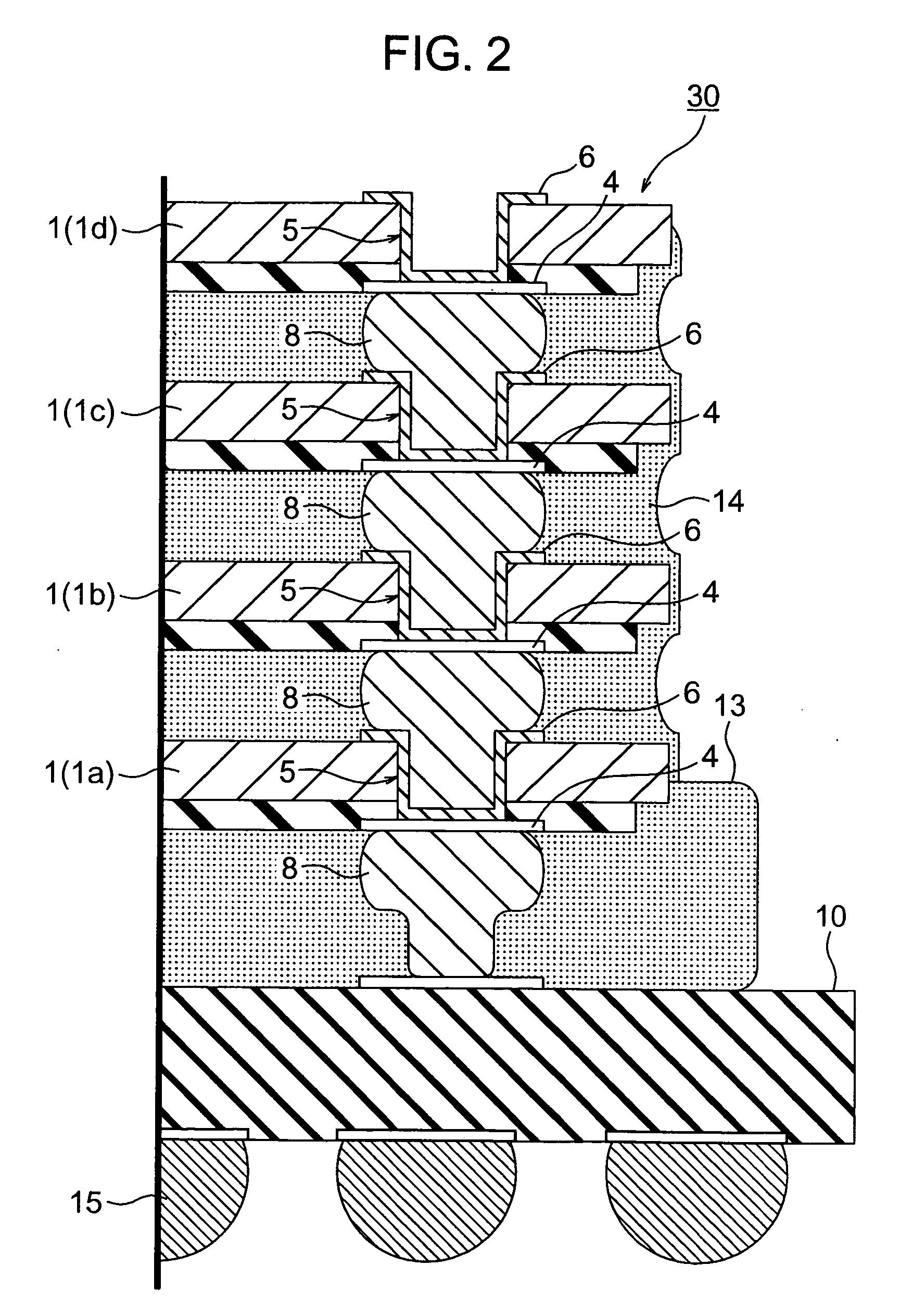
[0056]FIG. 2 is a schematic sectional view obtained by enlarging a part of FIG. 1.

[0057]FIG. 3 is a schematic sectional view showing a schematic configuration of the semiconductor chip in FIG. 1.

[0058]FIG. 4 is a schematic sectional view obtained by enlarging a part of FIG. 3.

[0059] FIGS. 5 to 10 are illustrations for explaining fabrication of a semiconductor chip in fabrication of a semiconductor device (A is a schematic top view and B is a schematic sectional view).

[0060] FIGS. 11 to 14 are schematic sectional views for explaining an assembling process in fabrication of a semiconductor device.

[0061] As shown in FIG. 1, the semiconductor device of this embodiment 1 has a package structure having a chip laminated body 30 constituted of a plurality of semiconductor chip...

embodiment 2

[0109]FIGS. 16 and 17 are schematic sectional views for explaining fabrication of a semiconductor chip in fabrication of a semiconductor device of embodiment 2 of the present invention.

[0110] As a method for covering the inner wall surface of a through-hole 5 with an insulating film 24, an example is described in which the inner-wall surface of the through-hole 5 is covered with the insulating film 24 by forming the thin insulating film 24 along the inner-wall surface of the through-hole 5 in the case of the above embodiment 1. In the case of this embodiment 2, an example is described in which the inside of the through-hole 5 is once filled with an insulating film 5 to cover the inner-wall surface of the through-hole 5 with the insulating film 24.

[0111] First, after forming the through-hole 5, the insulating film 24 made of a silicon oxide film is formed on the entire surface of the back 20y of a semiconductor wafer 20 through, for example, the plasma CVD method as shown in FIG. 1...

embodiment 3

[0115]FIG. 18 is a schematic sectional view for explaining an assembling process in fabrication of a semiconductor device of embodiment 3 of the present invention.

[0116] In the case of the above embodiment 1, an example is described in which the lowest-stage semiconductor chip 1 (1a) is mounted on the principal plane of the wiring board 10 through the adhesive 13 and then three semiconductor chips (1b, 1c, and 1d) are successively laminated on the lowest-stage semiconductor chip (1a) to form the chip lamination body 30. Thereafter, the chip lamination body 30 is mounted on the principal plane of the wiring board 10. The chip lamination body 30 is mounted by compression-bonding the chip lamination body 30 to the wiring board 10 while setting the adhesive 13 between the semiconductor chip 1 (1a) and the wiring board 10.

[0117] Also in the case of this embodiment 3, advantages same as those of the above embodiment 1 are obtained.


PUM


Abstract

To provide a very-low-cost and short-TAT connection structure superior in connection reliability in accordance with a method for three-dimensionally connecting a plurality of semiconductor chips at a shortest wiring length by using a through-hole electrode in order to realize a compact, high-density, and high-function semiconductor system. The back of a semiconductor chip is decreased in thickness up to a predetermined thickness through back-grinding, a hole reaching a surface-layer electrode is formed at a back position corresponding to a device-side external electrode portion through dry etching, a metallic deposit is applied to the sidewall of the hole and the circumference of the back of the hole, a metallic bump (protruded electrode) of another semiconductor chip laminated on the upper side is deformation-injected into the through-hole by compression bonding, and the metallic bump is geometrically caulked and electrically connected to the inside of a through-hole formed in an LSI chip. It is possible to realize a unique connection structure having a high reliability in accordance with the caulking action using the plastic flow of a metallic bump in a very-low-cost short-TAT process and provide a three-dimensional inter-chip connection structure having a high practicability.

Description

BACKGROUND OF THE INVENTION [0001] The present invention relates to a semiconductor device having a plurality of semiconductor chips three-dimensionally laminated. PRIOR ART [0002] In recent years, a system-in-package technique has been noticed which mounts a plurality of semiconductor chips on which integrated circuits are mounted at a high density to realize an advanced-function system in a short period and various mounting structures are proposed from various companies. Particularly, development of a laminated package which is able to three-dimensionally laminate a plurality of semiconductor chips and realize great downsizing. [0003] Because wire bonding is mainly used for electrical connection between a semiconductor chip and a mounting substrate, it is necessary to make an upper-stage semiconductor chip to be laminated smaller than a lower-stage semiconductor chip to be laminated. When laminating semiconductor chips having the same size, it is necessary to secure a wire bonding...

Claims


Application Information

Patent Timeline
Patent Type & Authority Applications(United States)
IPC IPC(8): H01L23/12H01L21/56H01L21/60H01L23/31H01L23/48H01L23/485H01L23/495H01L25/065H01L25/07H01L25/18
CPCH01L21/563H01L24/13H01L23/481H01L25/0657H01L25/50H01L2224/1134H01L2224/13144H01L2224/16145H01L2224/16225H01L2224/16237H01L2224/73203H01L2224/83102H01L2224/83192H01L2224/92125H01L2225/06513H01L2225/06541H01L2924/01005H01L2924/01013H01L2924/01022H01L2924/01029H01L2924/01075H01L2924/01078H01L2924/01079H01L2924/14H01L2924/15311H01L2924/19041H01L2924/30105H01L2924/30107H01L2924/3011H01L23/3128H01L24/11H01L2224/73104H01L24/83H01L2224/73204H01L2224/32225H01L2224/32145H01L24/29H01L2924/014H01L2924/00013H01L2924/01006H01L2924/01033H01L2924/00014H01L2224/13099H01L2924/00H01L24/05H01L24/06H01L24/16H01L2224/05001H01L2224/05022H01L2224/05147H01L2224/05166H01L2224/0557H01L2224/05572H01L2224/05644H01L2224/05647H01L2224/06181H01L2224/11H01L2224/13025H01L2224/16146H01L2224/17181H01L2924/181H01L2924/351H01L2224/13
Inventor TANAKA, NAOTAKANAKAZATO, NORIONAITO, TAKAHIRO
Owner RENESAS TECH CORP
Why Eureka
Try Eureka