Method of manufacturing a micro-electrical-mechanical system

a manufacturing method and micro-electrical technology, applied in the direction of microstructural devices, acceleration measurement using interia forces, coatings, etc., can solve the problems of low yield, undesirable long and complex manufacturing methods, and beams that are vulnerable to damag

Inactive Publication Date: 2005-12-01
LAPIS SEMICON CO LTD
View PDF10 Cites 26 Cited by
  • Summary
  • Abstract
  • Description
  • Claims
  • Application Information

AI Technical Summary

Benefits of technology

[0013] During the dicing process, since the moving member is immobilized by the sacrificial layer, it cannot stress or damage the microstructure by moving, and the beams, if present, are also reinforced by the sacrificial layer for further protection from stress and damage. This protection is attained without the need to form and then remove a separate reinforcing layer. The sacrificial layer may be removed from the beams by the etching process that frees the moving member from the frame.

Problems solved by technology

The need to apply a polyimide reinforcing film and then remove the film individually from each chip after dicing makes this manufacturing method undesirably lengthy and complex.
A further problem is low yield, because despite the reinforcement, the beams are vulnerable to damage during the dicing process.
The manufacturing cost per chip is accordingly comparatively high.

Method used


Image

  • Method of manufacturing a micro-electrical-mechanical system
  • Method of manufacturing a micro-electrical-mechanical system
  • Method of manufacturing a micro-electrical-mechanical system

Examples


first embodiment

[0033] The adhesive sheet in the first embodiment is a so-called UV sheet. The term UV sheet is used herein to denote a flat sheet made of a base material such as polyester, having on one surface an adhesive substance, the adhesive strength of which is weakened by exposure to ultraviolet (UV) light.

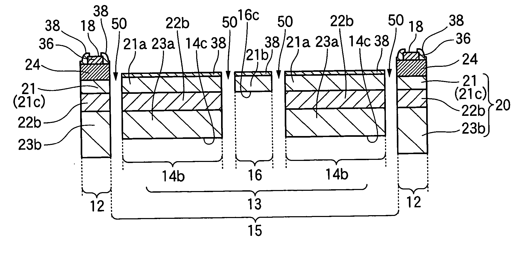
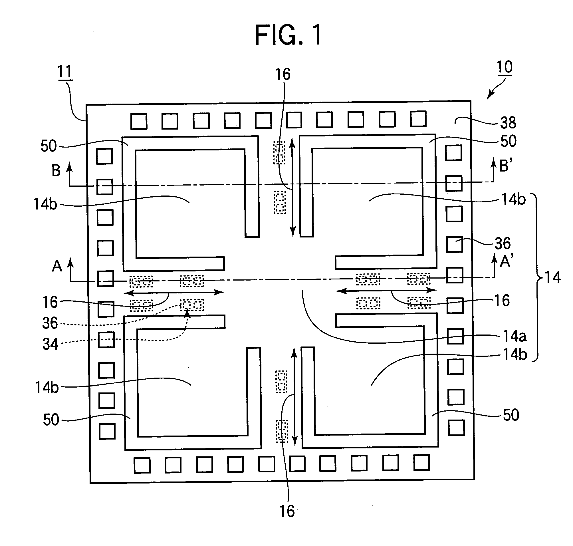
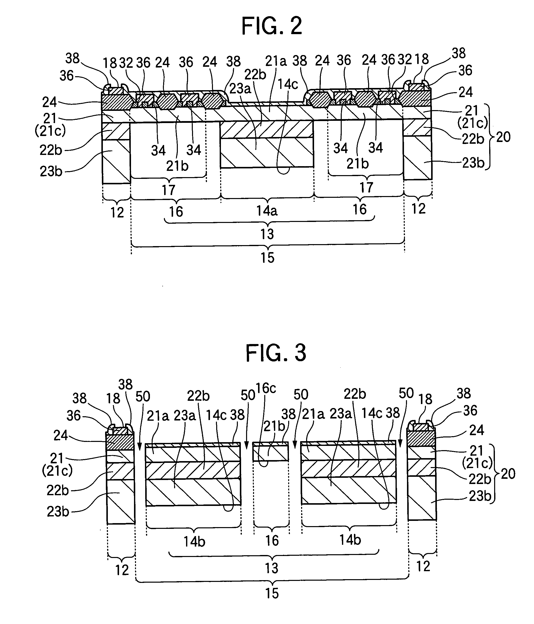
[0034] Two slightly different fabrication methods conforming to the first embodiment will be described with reference to FIGS. 5 to 18. These drawings show one representative acceleration sensor among the plurality of acceleration sensors that are simultaneously fabricated in a single wafer substrate. Each acceleration sensor 10 has the exemplary structure shown in FIGS. 1-4.

[0035] Both fabrication methods start from a semiconductor substrate 20 having a first major surface 20a (defined as the front surface or upper surface) and a second major surface 20b (defined as the back surface or lower surface) as shown in FIG. 5. The semiconductor substrate 20 comprises a sacrificial layer 22 sa...

second embodiment

[0070] The second embodiment replaces the UV sheet used in the first embodiment with a so-called thermal release sheet. The thermal release sheet is an adhesive sheet having an adhesive that weakens when heated to a predetermined temperature, so that the sheet peels away easily from the object to which it is attached. In other respects, the second embodiment is similar to the first embodiment.

[0071] A first fabrication method according to the second embodiment of the invention will now be described. In the first fabrication method, after the precursor microstructure 13a has been formed, the semiconductor substrate 20 is secured to an adhesive sheet of the thermal release type and diced into chips; then the microstructure in each chip is completed by removing the sacrificial layer, after which the adhesive sheet is heated and peeled off. All processes preceding the attachment of the adhesive sheet are substantially the same as in the first embodiment, so detailed descriptions will b...


PUM

PropertyMeasurementUnit
sizesaaaaaaaaaa
temperatureaaaaaaaaaa
pressureaaaaaaaaaa

Abstract

Micro-electrical-mechanical systems are fabricated in a substrate having a sacrificial layer sandwiched between two semiconductor layers. The semiconductor layers are selectively etched to create non-etched frames and etched microstructures immobilized within the frames by the sacrificial layer. An adhesive sheet is attached to one surface of the substrate, and the substrate is diced into chips, each including one frame and one immobilized microstructure. The sacrificial layer is then selectively etched to free a movable member in each microstructure. Finally, the chips are detached from the adhesive sheet, each chip becoming a micro-electrical-mechanical system. This fabrication method provides a simple and inexpensive way to avoid damage to the microstructure during the dicing process.

Description

BACKGROUND OF THE INVENTION [0001] 1. Field of the Invention [0002] The present invention relates to a method of manufacturing a micro-electrical-mechanical system. [0003] 2. Description of the Related Art [0004] It is known art to use semiconductor fabrication techniques in micro-machining processes that create structures with sizes on the order of a few hundred micrometers. Applications of this technology are beginning to appear in sensors, optical communication switches, radio-frequency (RF) devices, and other areas. [0005] Because these tiny structures can be manufactured by conventional semiconductor fabrication processes, they can be integrated together with signal processing circuitry, for example, onto a single chip. Chips of this type, which combine electronics with mechanics, are known as micro-electrical-mechanical systems (MEMS), and the technology they embody is known as microsystem technology (MST). The chips will be referred to as MEMS devices below. [0006] Accelerati...

Claims


Application Information

Patent Timeline
Patent Type & Authority Applications(United States)
IPC IPC(8): B81B3/00G01P15/12B81C1/00H01L21/00H01L21/301H01L29/84
CPCB81C1/00896B81B7/02
Inventor IKEGAMI, NAOKATSU
Owner LAPIS SEMICON CO LTD
Why Eureka
Try Eureka