Vertical semiconductor devices or chips and method of mass production of the same

a technology of semiconductor chips and semiconductor chips, applied in the direction of semiconductor devices, basic electric elements, electrical equipment, etc., can solve the problems of increasing the chance of damaging the epitaxial layer of leds, reducing the throughput, and high cost of laser lift-off equipment, etc., to achieve fast heat dissipation, high cost, and complex process

Inactive Publication Date: 2005-12-08
PENG HUI +1
View PDF6 Cites 16 Cited by
  • Summary
  • Abstract
  • Description
  • Claims
  • Application Information

AI Technical Summary

Benefits of technology

[0019] 7. The vertical semiconductor chips or devices of the present invention have all of the advantages of flip chip technique, such as the fast heat dissipation, and without its disadvantage, such as the complex process, expensive equipments, and low throughput.
[0020] The primary object of the present invention is to provide methods for massively manufacturing vertical semiconductor chips or devices, including GaN, GaInP, and GaInNP based LEDs, with high crystal quality, lower cost, higher throughput, and high yield.
[0021] The second object of the present invention is to provide vertical semiconductor chips or devices, including high power GaN, GaInP, and GaInNP based LEDs, with better uniformity of wavelength and intensity of emitting light over whole epitaxial wafer.
[0022] The third object of the present invention is to provide vertical semiconductor chips or devices, including high power GaN, GaInP, and GaInNP based LEDs, with higher crystal quality of epitaxial layers by removing the original substrate before growing active layers.
[0023] The fourth object of the present invention is to provide vertical semiconductor chips or devices, including high power GaN, GaInP, and GaInNP based LEDs, with better ESD property.
[0024] The fifth object of the present invention is to provide vertical semiconductor chips or devices, including high power GaN, GaInP, and GaInNP based LEDs, with better extraction efficiency by eliminating totally internal reflections for GaN and GaInNP based LEDs and by eliminating the absorption of an original substrate for GaInP based LEDs.

Problems solved by technology

It may be needed for laser beam to scan an epitaxial wafer more than one times, which decreases the throughput and increases the chance of damaging the epitaxial layer of LEDs.
Also the laser lift-off equipment is expensive.
To grow a thick semiconductor substrate in this way, however, is very expensive.
Also semiconductor devices or chips grown on the so-obtained semiconductor substrate do not have the advantages of flip chip technique.
Substrate temperature non-uniformity may result in deviation from target wavelength and intensity of emitted light.
As a consequences, the composition and quality of disposed epitaxial layer over the substrate is not uniform.
Therefore, LED chips on an about 5 mm ring from the edge of the substrate are not qualified, i.e., the yield is lower.
Therefore the different in the thermal expansion coefficients of the original substrate and the epitaxial layer causes a stress which affects the crystal quality of the epitaxial layer.

Method used


Image

  • Vertical semiconductor devices or chips and method of mass production of the same
  • Vertical semiconductor devices or chips and method of mass production of the same
  • Vertical semiconductor devices or chips and method of mass production of the same

Examples


first embodiment

FIG. 2a to 2g

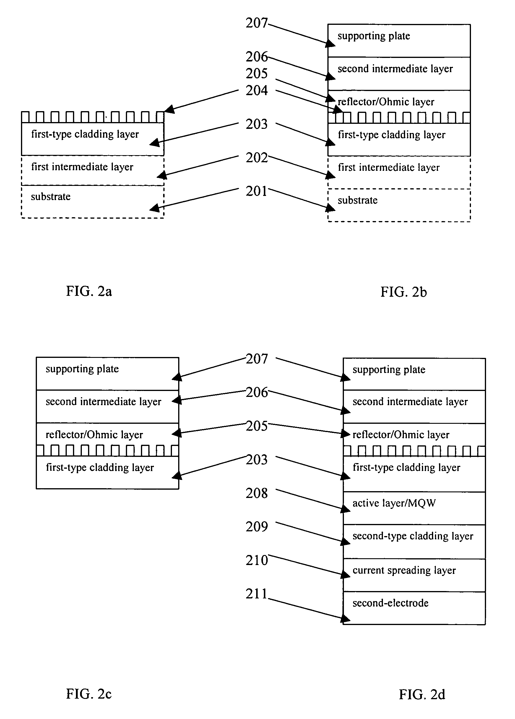
[0055] The selections of a structure and a material of first intermediate layer 202 depend on the selection of both a substrate removing process and a material of substrate 201. For different substrate removing processes, the structure and material of first intermediate layer 202 are different

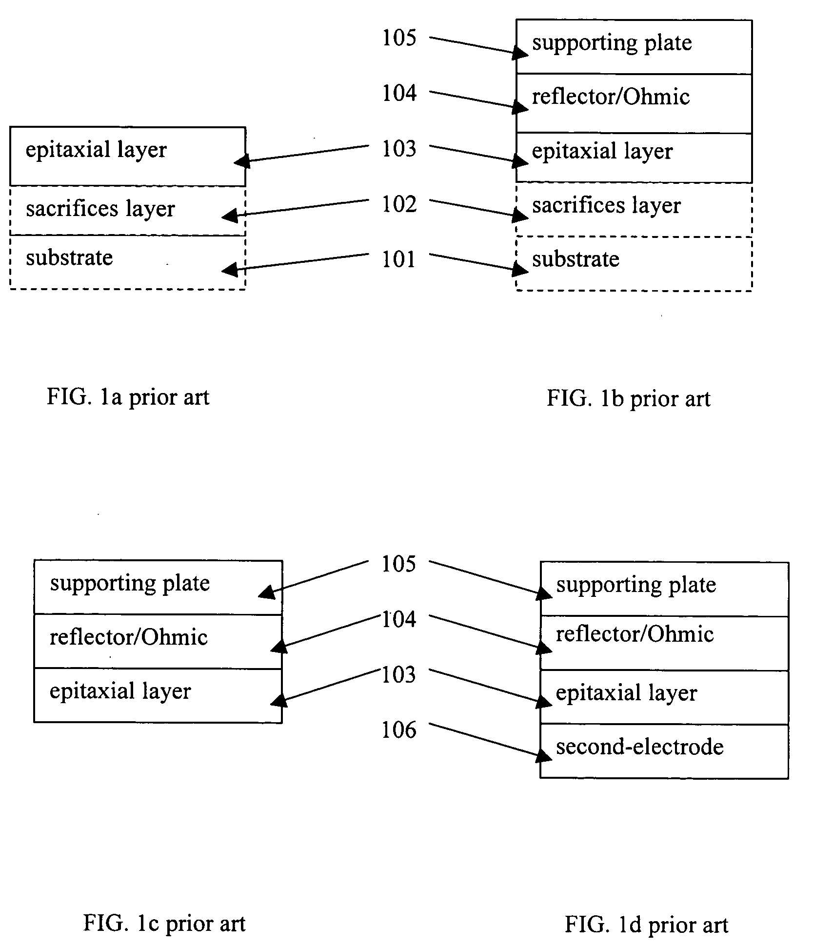
[0056] For GaN based LEDs, a common choice of substrate 201 is a sapphire substrate. Two processes to remove sapphire substrate 201 are disclosed.

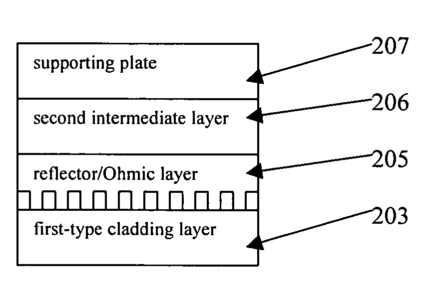
[0057] The first sapphire substrate removing process is to remove both sapphire substrate 201 and first intermediate layer 202 by precisely lapping / polishing before growing an epitaxial layer comprising an active layer. First intermediate layer 202 comprises one or multiple buffer layers. First-type cladding layer 203 is grown on the top of the buffer layers, and preferably is an n-type cladding layer. Textured top surface 204 of first-type cladding layer 203 is formed by either dry or wet etching (details is disclosed in FIG. 4) for s...

third embodiment

FIG. 3a to FIG. 3d

[0070] For GaN based LEDs, first intermediate layer 302 serves as a buffer layer comprising AlN and GaN buffer layers growing on the (111) plane of Si substrate 301. To grow AIN, firstly, chemically clean polished Si substrate 301. Secondly, growing AlN single crystalline layer at 1100-1250 degree C. for thickness of about 100-200 nm and obtaining smooth and featureless surface. Thirdly, growing GaN buffer layer at temperature of 1050 degree C. Then first-type cladding layer 303 is grown on GaN buffer layer.

[0071] The process steps of texturing the top surface of first-type cladding layer 303, disposing reflector / Ohmic layer 305, disposing second intermediate layer 306, disposing supporting plate 307, removing Si substrate 301 and first intermediate layer 302, disposing a first-type cladding thin film of first-type cladding layer 303, growing active layer 3308 and second-type cladding layer 309, disposing current spreading layer 310 and patterned second-electrode...

fourth embodiment

FIG. 3e

[0073] An n-type AlGaN thin film (for example, Al.sub.0.07Ga.sub.0.93N having an electron density of 3.times.10.sup.17 / cm.sup.3), as a first-type cladding layer 303, may be directly grown (at about 1000 degree C.) on Si substrate 301. The rest process steps, starting with the process steps of texturing the top surface of first-type cladding layer 303 to the process step of disposing patterned second-electrode, are the same as that of the first embodiment of FIG. 3a to FIG. 3d.

[0074]FIG. 4a is a top view of textured top surface 400 formed by etching the top surface of first-type cladding layers 203 or 303 respectively. Textured top surface 400 comprises two types: mesa-type and well-type.

[0075]FIG. 4b is a cross sectional view of an embodiment of mesa-type textured top surfaces 400. Textured top surface 400 has mesa 402a and well-separator 401a, it is preferred to form mesa 402a having the same dimension as that of a semiconductor devise or chip, and to form well-separator ...


PUM


Abstract

The vertical semiconductor chips or devices have all of advantages of flip chip technique and without its disadvantages. The present invention discloses methods of mass production of the vertical semiconductor chips or devices comprising GaN, GabInP, and GaInNP based LEDs with higher crystal quality, higher throughput, higher yield, and lower cost. The methods comprise the following process steps in the order presented: growing a first-type cladding layer, disposing a reflector/Ohmic layer, disposing a second intermediate layer, disposing an electrically conductive supporting plate, removing the original substrate and the first-type cladding layer exposed, growing an epitaxial layer comprising an active layer and a second-type cladding layer, disposing a second-electrode, and dicing into individual dies.

Description

BACKGROUND OF THE INVENTION [0001] (1) Field of the Invention [0002] The present invention relates to vertical semiconductor chips or devices including GaN, GaInP, and GaInNP based LEDs, especially for high power LEDs, and methods of mass production of the same. [0003] (2) Prior Art [0004] There are varieties of prior art discussing vertical semiconductor devices or chips and method of manufacturing the same. Main advantages associated with the vertical structure comprise the following: (1) vertical semiconductor devices or chips have all of advantages of flip chip technique including fast heat dissipation and without its disadvantages, such as complex process steps, low throughput, and expensive equipments; (2) two electrodes are on the two opposite sides of a vertical semiconductor device or chip and, thus, current distributes more uniformly, current density is higher, ESD property is improved. [0005] U.S. Pat. No. 6,320,206 by Coman, et al. disclosed methods for removing sapphire...

Claims


Application Information

Patent Timeline
Patent Type & Authority Applications(United States)
IPC IPC(8): H01L21/00H01L21/20H01L21/461H01L33/00H01L33/22H01L33/40
CPCH01L21/02381H01L21/0242H01L21/02458H01L33/405H01L21/0254H01L33/0079H01L33/20H01L21/02505H01L33/0093
Inventor PENG, HUILUO, WEI
Owner PENG HUI
Why Eureka
Try Eureka