

Low thermal resistance light emitting diode
a light-emitting diode, low-temperature technology, applied in the direction of basic electric elements, electrical equipment, semiconductor devices, etc., can solve the problems of excessive thermal resistance, limited thermal resistance, and high so as to reduce the thickness of the package, reduce the production cost of led packages, and reduce the thermal resistance of led packages
- Summary
- Abstract
- Description
- Claims
- Application Information
AI Technical Summary
Benefits of technology
Problems solved by technology
Method used
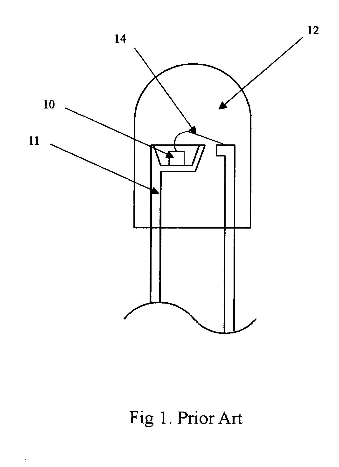
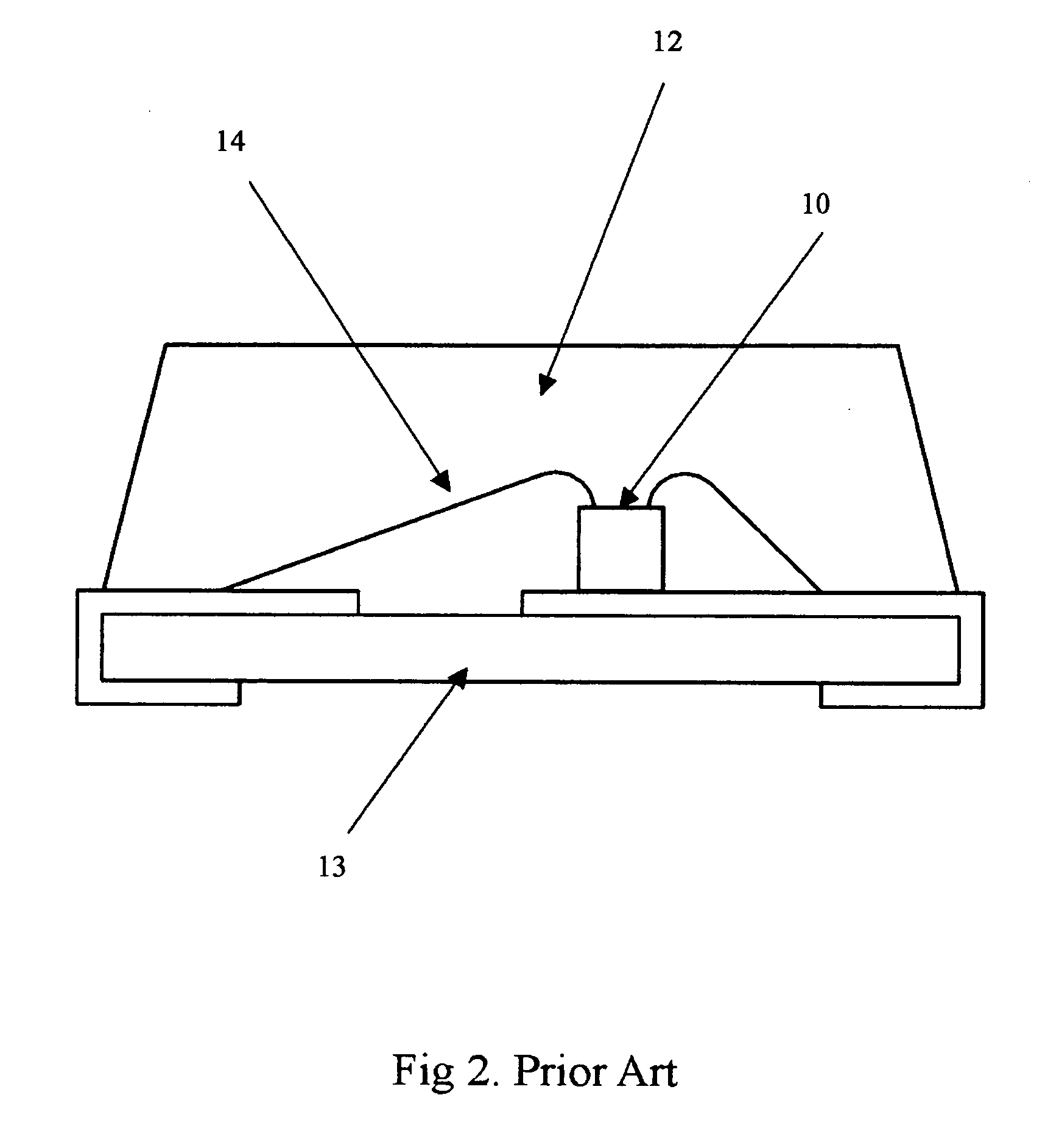
Image

Examples
first embodiment
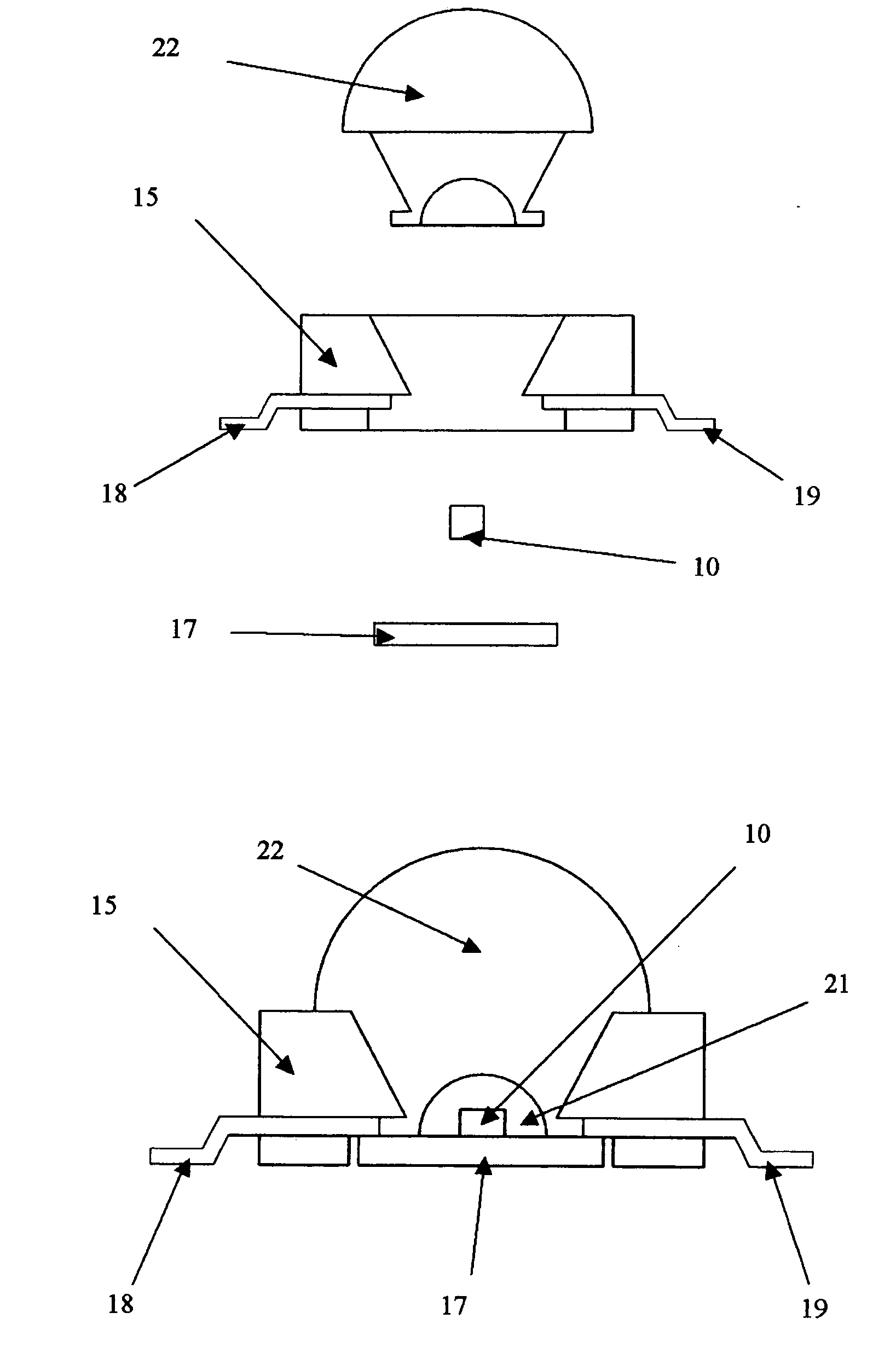
[0028]FIG. 5 shows the present invention. A metal sheet is punched out by a press into two lead frames for positive lead 18 and negative lead 19. The lead frames are embedded in a mold of insulating epoxy 15. The positive lead frame 18 and the negative lead frame are exposed inside the core or cavity of the mold 15. A plastic transparent lens 22 is mounted on top of the cavity 15 using transfer molding. The lens typical has at least transmission coefficient of 70% at a wavelenth of 550 nm. The lead frames 18 and 19 have exposed sections without insulating covering. The bottom of the mold 15 has a recess, which overlays a silicon submount 17. A LED chip 10 is flip chip mounted on the submount 17 inside the recess. The submount 17 has printed wirings on it, to which the exposed sections of the lead frames 18 and 19 are soldered with Pb / Sn solder paste, forming connections to the two bottom electrodes of the LED chip 10 without bonding wire. The LED chip 10 is covered with silicon glue...
second embodiment
[0029]FIG. 6 shows the present invention. A metal sheet is punched out by a press into two lead frames for positive lead 18 and negative common lead 19. The lead frames are exposed inside the cavity of the mold 15. The bottom of the mold 15 has an opening, which overlays an aluminum oxide submount 17. The submount 17 has printed wirings, to which the lead frames 18 and 19 are soldered with solder paste, forming connections to the two bottom electrodes of the LED chip 10 without wire bonding. The LED chip 10 is covered with silicon glue to form wireless bonding with low thermal resistance and high reliability. Other back-filling material such as epoxy, glass, Teflon may also be used, so long as the refractive index is greater than 1.3 and the transmission coefficient is greater than 80%.
third embodiment
[0030]FIG. 7 shows the present invention. A metal sheet is punched out by a press as three positive terminal lead frames and one common negative terminal lead frame. These lead frames are imbedded in insulating mold 15 by means of injection molding. The three positive terminal lead frames 18 and the negative terminal lead frame 19 have exposed sections without insulating covering. A transparent lens 22 is mounted on top of the cavity of the mold 15 using transfer molding. The lens should have a transmission coefficient greater than 70% at a wavelength of 550 nm. The bottom of the mold 15 has a recess, which overlays a silicon submount 17. Three LEDs for emitting red, green and blue lights are mounted on the submount 17 and housed inside the recess. The submount has printed wirings, to which the exposed sections of the lead frames 18 and 19 are soldered, forming connections without wire bonding. The LED chips are covered with silicon glue to form wireless bonding with low thermal res...
PUM
 Abstract
Description
Claims
Application Information