Protected organic electronic devices and methods for making the same

a technology of organic electronic devices and shielded organic materials, applied in the direction of discharge tube/lamp details, organic semiconductor devices, discharge tube luminescnet screens, etc., can solve the problems of easy creases or dent in thin metal foils, damage, or even destroy, display damage, etc., to achieve high strength and resistance. , the effect of high resolution

Inactive Publication Date: 2005-12-08
UNIVERSAL DISPLAY
View PDF22 Cites 114 Cited by
  • Summary
  • Abstract
  • Description
  • Claims
  • Application Information

AI Technical Summary

Benefits of technology

[0010] According to a first aspect of the invention, top-emitting, high-resolution, OLED structures are provided which include a metal foil substrate and a planarization layer disposed over the metal foil substrate. Metal foils have a number of desirable properties, including high strength and resistance to shrinkage and distortion, which make them ideal as substrates for the formation of hi

Problems solved by technology

However, various issues can arise when using thin substrates.
In addition, thin metal

Method used


Image

  • Protected organic electronic devices and methods for making the same
  • Protected organic electronic devices and methods for making the same
  • Protected organic electronic devices and methods for making the same

Examples


Embodiment Construction

[0018] The present invention now will be described more fully hereinafter, in some instances with reference to the accompanying drawings in which certain preferred embodiments of the invention are shown. This invention may, however, be embodied in different forms and should not be construed as limited to the embodiments set forth herein.

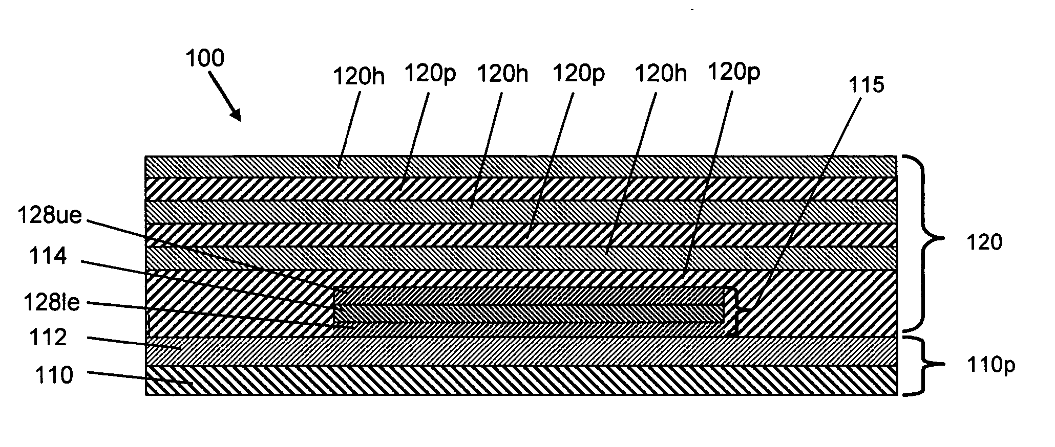
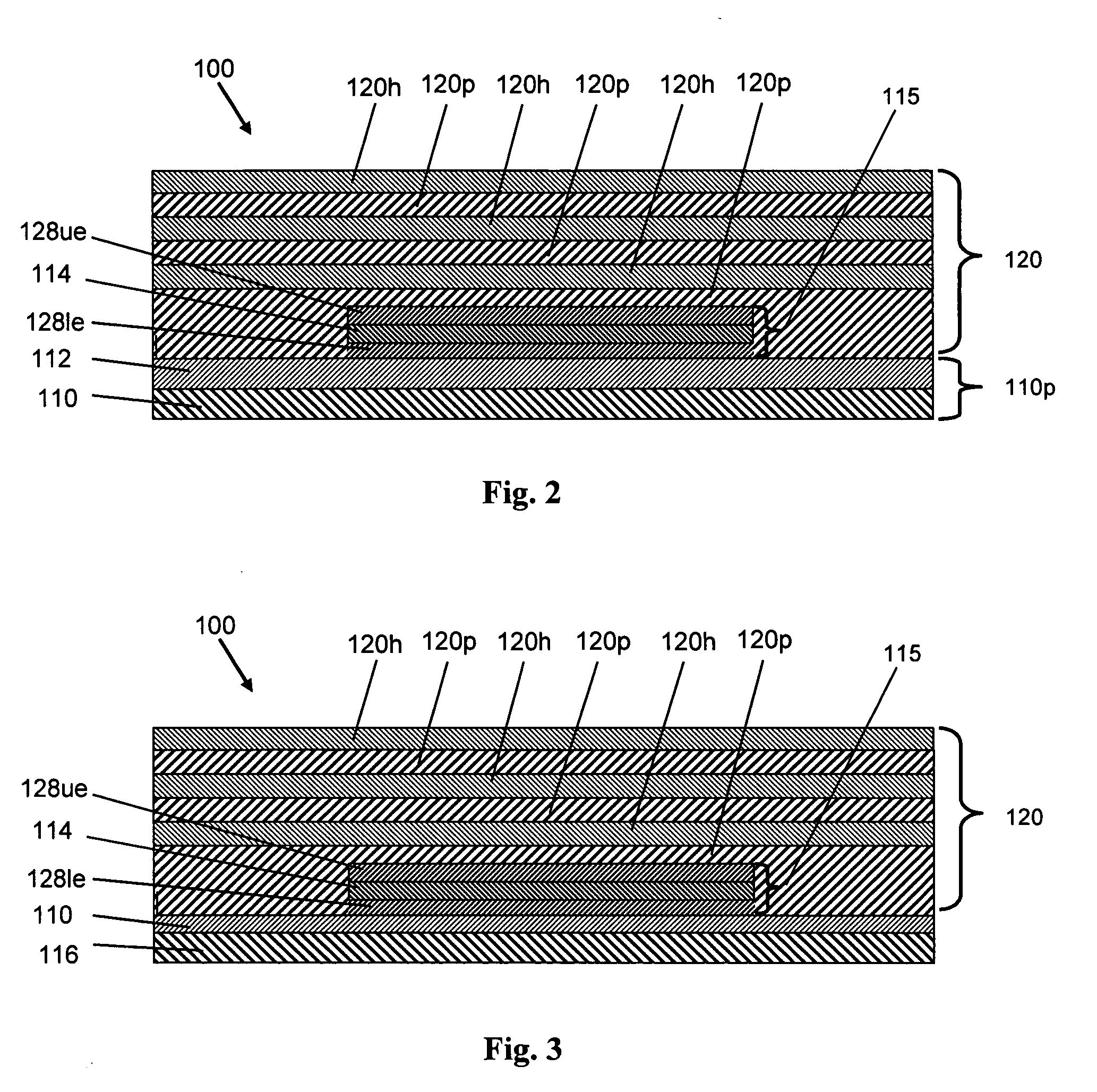
[0019] As noted above, OLED devices, including the various OLED devices of the present invention, typically include a substrate region, an OLED stack over the substrate region, and an upper barrier region over the OLED stack to protect the OLED stack from environmental species such as water and oxygen. An “OLED stack” includes lower and upper electrodes (i.e., an anode and a cathode) as well as the region (including an organic layer) that is found between the electrodes. As discussed further below, a wide range of OLED stacks are known in the art.

[0020] As used herein, a “layer” of a given material includes a region of that material whose thickness...


PUM


Abstract

The present invention relates to structures and components for protecting organic light emitting diodes from environmental elements such as moisture and oxygen. According to a first aspect of the invention, top-emitting, high-resolution, OLED structures are provided which include a metal foil substrate; a planarization layer disposed over the metal foil substrate; an OLED stack (which includes lower and upper electrodes as well as an organic region disposed between the electrodes) disposed over the planarization layer; and a multilayer barrier region disposed over the OLED stack. A second aspect of the invention is directed to flexible, top emitting OLED structures which include the following: thin substrate region (i.e., a substrate having a thickness that is less than 200 microns); an OLED stack disposed over the flexible substrate region; a transparent upper barrier region that cooperates with the flexible substrate region to encapsulate the OLED stack, thereby protecting it from outside species such as water or oxygen; and a polymeric reinforcement layer which has a Young's Modulus ranging from about 0.3 to 7 GPa, which is disposed (i) below the substrate region, (ii) above the upper barrier region (in which case it is transparent), or (iii) both below the substrate region and above the upper barrier region.

Description

FIELD OF THE INVENTION [0001] The present invention relates to various novel organic light emitting diode (OLED) structures. BACKGROUND OF THE INVENTION [0002] Organic light emitting diodes (OLEDs) are becoming increasingly important from an economic standpoint. For example, OLEDs are potential candidates for a wide variety of virtual- and direct-view type displays, such as lap-top computers, televisions, digital watches, telephones, pagers, cellular telephones, calculators and the like. Unlike inorganic semiconductor light emitting devices, organic light emitting devices are generally simple and are relatively easy and inexpensive to fabricate. Also, OLEDs readily lend themselves to applications requiring a wide variety of colors and to large-area device applications. [0003] In general, two-dimensional OLED arrays for imaging applications are known in the art, and include a plurality of pixels arranged in rows and columns. FIG. 1A is a simplified schematic representation (cross-sec...

Claims


Application Information

Patent Timeline
IPC IPC(8): H01L27/32H01L51/52H05B33/00
CPCH01L27/3244H01L51/5237H01L51/5284Y02E10/549H01L2251/5338H01L51/0097H01L2251/5315H10K59/12H10K77/111H10K50/8445H10K50/865H10K2102/3026H10K2102/311
Inventor HACK, MICHAELCHWANG, ANNASILVERNAIL, JEFFREY ALAN
Owner UNIVERSAL DISPLAY
Why Eureka
Try Eureka