SOI chip with recess-resistant buried insulator and method of manufacturing the same

a technology of buried insulator and soi chip, which is applied in the direction of semiconductor devices, semiconductor/solid-state device details, electrical apparatus, etc., can solve the problems of exposed buried oxide layer and potentially affecting device reliability, and achieve the effect of enhancing device reliability and minimizing parasitic capacitan

Inactive Publication Date: 2005-12-15
TAIWAN SEMICON MFG CO LTD
View PDF60 Cites 15 Cited by
  • Summary
  • Abstract
  • Description
  • Claims
  • Application Information

AI Technical Summary

Benefits of technology

[0010] The present invention describes embodiments of an improved method of fabricating strained-silicon-on-insulator substrates. In one embodiment, a recess-resistant film is used with the buried insulator to prevent erosion of the buried insulator during subsequent processing steps. For example, the recess-resistant film can be a silicon nitride film, which etches ten times more slowly than silicon oxide for common wet etch processes.
[0014] Aspects of the present invention provide advantages over prior art devices. For example, the buried insulating layer will not include recesses. This feature helps to minimize parasitic capacitance between the substrate and metal lines running over the device. This feature minimizes any concentration of electric field lines around the exposed comers of the silicon mesas and therefore enhance device reliability.

Problems solved by technology

One problem of the mesa isolation is that the exposed buried oxide layer 112 surface will be recessed in subsequent chemical treatments such as wafer cleaning steps.
This recess is illustrated in FIG. 2b. The recessed buried oxide results in a number of problems.
It also leads to a concentration of electric field lines around the exposed comers of the silicon mesas, which potentially impact device reliability.

Method used


Image

  • SOI chip with recess-resistant buried insulator and method of manufacturing the same
  • SOI chip with recess-resistant buried insulator and method of manufacturing the same
  • SOI chip with recess-resistant buried insulator and method of manufacturing the same

Examples


Embodiment Construction

[0027] The making and using of the presently preferred embodiments are discussed in detail below. It should be appreciated, however, that the present invention provides many applicable inventive concepts that can be embodied in a wide variety of specific contexts. The specific embodiments discussed are merely illustrative of specific ways to make and use the invention, and do not limit the scope of the invention.

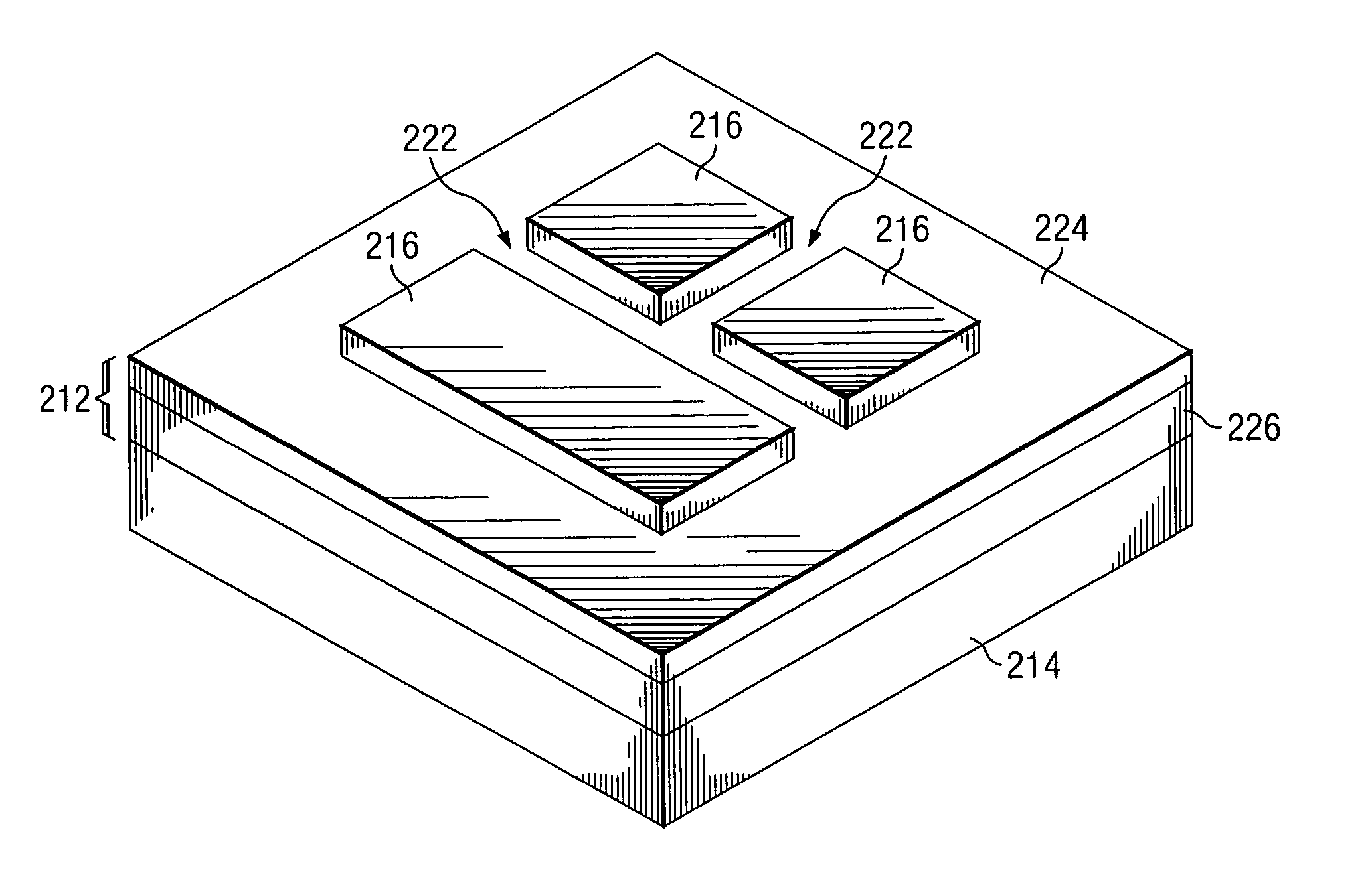
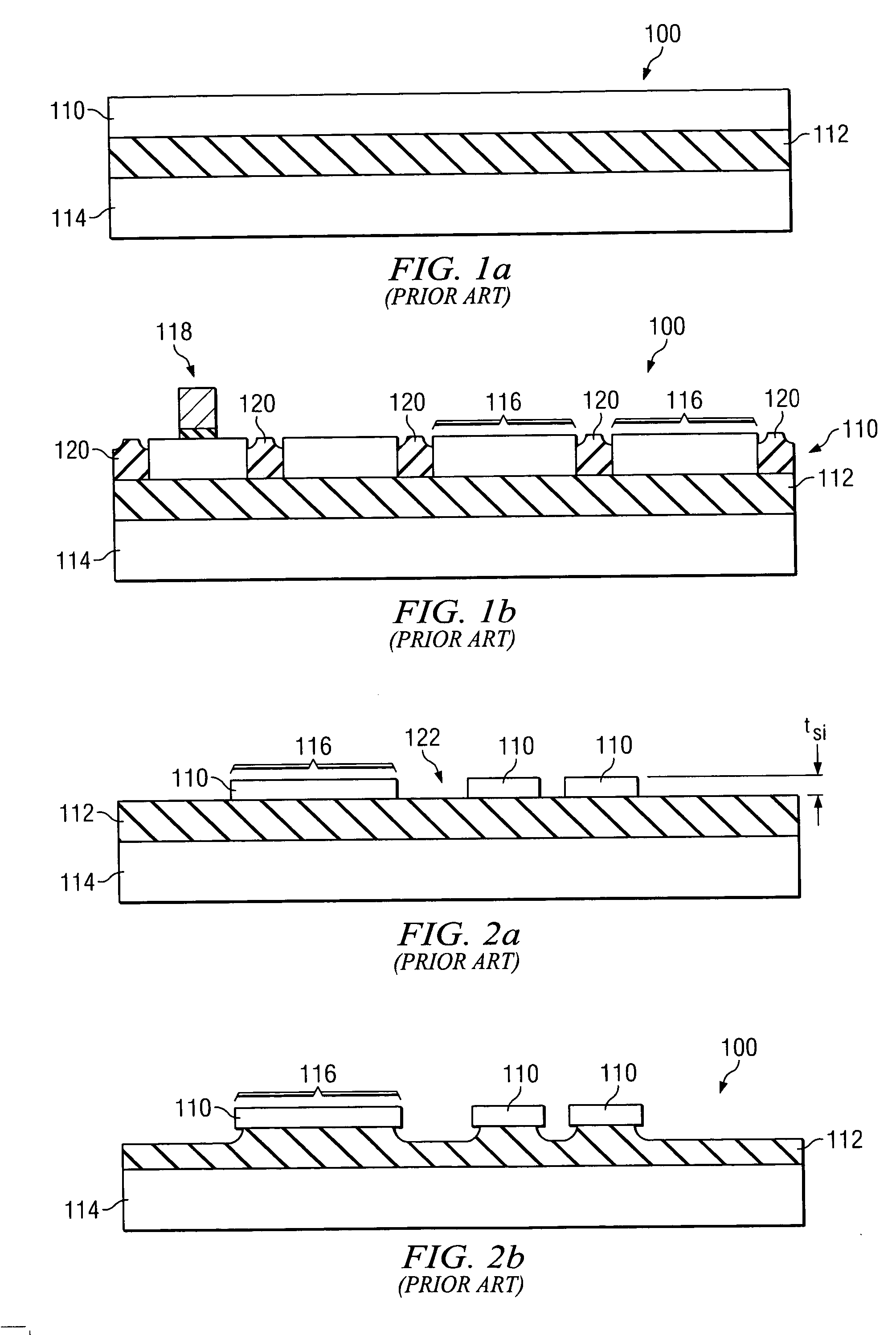
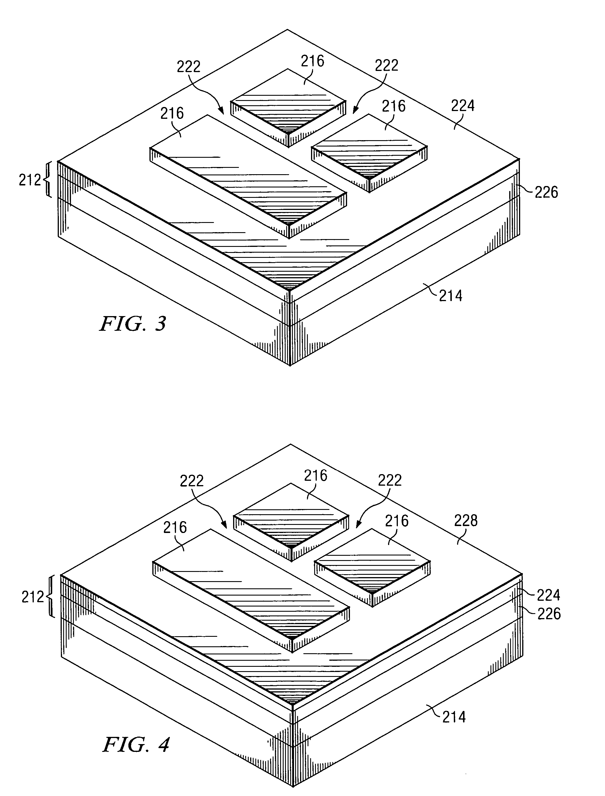
[0028] Aspects of the present invention relate generally to semiconductor materials, and more particularly to semiconductor-on-insulator substrates with a recess-resistant layer. Aspects of the present invention are also related to the manufacture of metal oxide semiconductor field effect transistors on semiconductor-on-insulator substrates with a recess-resistant layer.

[0029] According to the preferred embodiment of the present invention, a recess-resistant layer is provided in the buried insulator stack of a semiconductor-on-insulator wafer for the purpose of restricting...


PUM


Abstract

A semiconductor-on-insulator structure includes a substrate and a buried insulator stack overlying the substrate. The buried insulator stack includes a first dielectric layer and a recess-resistant layer overlying the first dielectric layer. A second dielectric layer can overlie the recess-resistant layer. A semiconductor layer overlying the buried insulator stack. Active devices, such as transistors and diodes, can be formed in the semiconductor layer.

Description

CROSS-REFERENCE TO RELATED APPLICATIONS [0001] This application is a divisional of patent application Ser. No. 10 / 384,859, entitled “SOI Chip With Recess-Resistant Buried Insulator And Method Of Manufacturing The Same,” filed on Mar. 10, 2003, which application is incorporated herein by reference. [0002] The present invention is related to commonly-assigned U.S. Pat. No. 6,911,379 B2, entitled “Method of Forming Strained Silicon on Insulator Substrate,” issued Jun. 28, 2005 (Attorney Docket No. TSMC2002-1384), which patent is incorporated herein by reference as if repeated in its entirety.TECHNICAL FIELD [0003] The present invention relates generally to semiconductor materials, and more particularly to semiconductor-on-insulator substrates with a recess-resistant layer. BACKGROUND [0004] Traditional silicon-on-insulator (SOI) integrated circuits are formed on SOI substrates. A cross-section of a silicon-on-insulator (SOI) substrate 100 is illustrated in FIG. 1a. SOI substrates typic...

Claims


Application Information

Patent Timeline
Patent Type & Authority Applications(United States)
IPC IPC(8): H01L21/20H01L21/31H01L21/762H01L21/84H01L27/01H01L27/12
CPCH01L21/76254H01L21/84H01L27/1203
Inventor YEO, YEE-CHIAHU, CHENMING
Owner TAIWAN SEMICON MFG CO LTD
Why Eureka
Try Eureka