

Optical module device
a technology of optical modules and optical modules, applied in the direction of radio frequency controlled devices, instruments, semiconductor lasers, etc., can solve the problems of inability to structure, device properties may deteriorate, and it is difficult to electrically separate the ground sid
- Summary
- Abstract
- Description
- Claims
- Application Information
AI Technical Summary
Problems solved by technology
Method used
Image

Examples
first embodiment
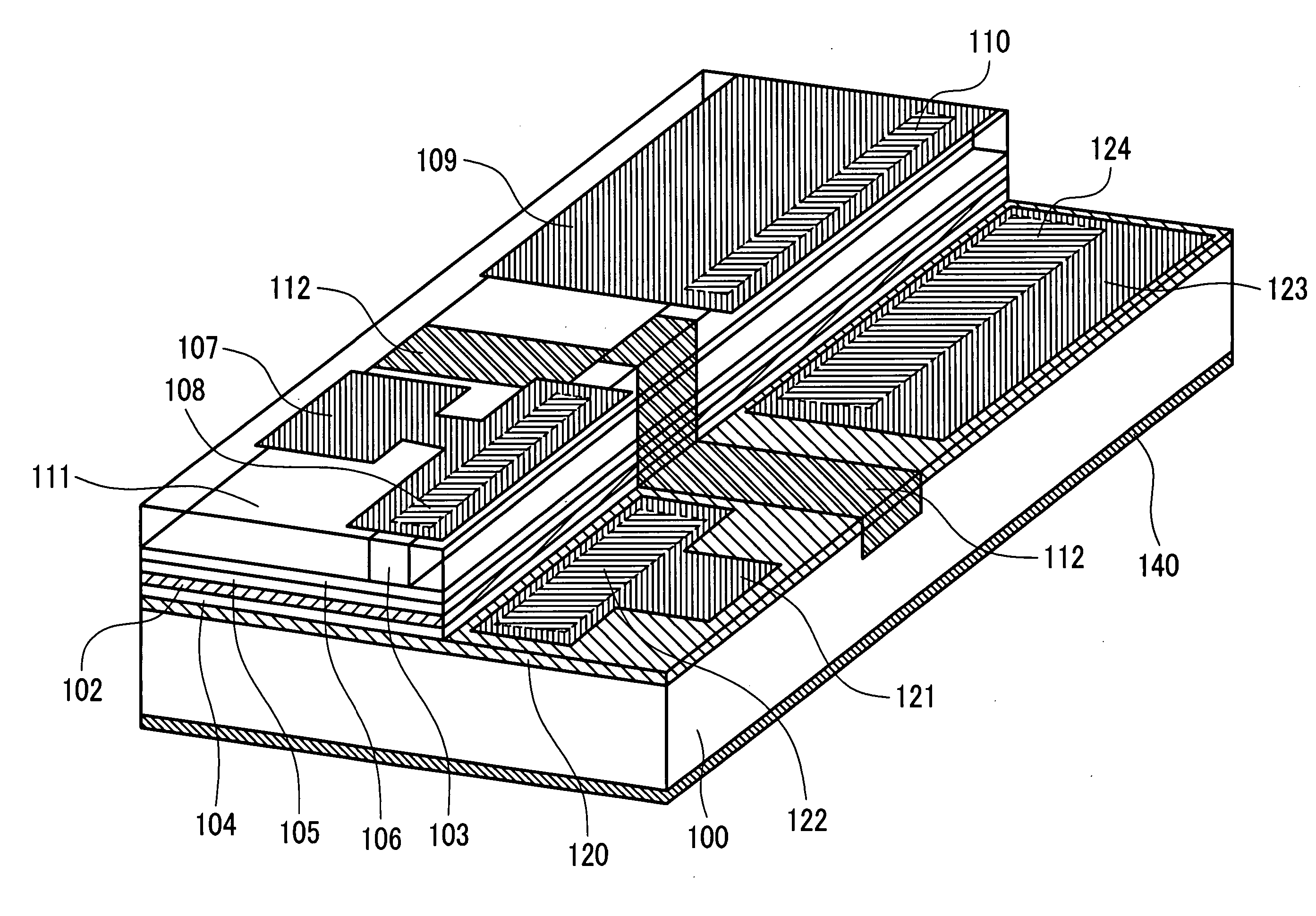
[0037]FIG. 6 is an oblique perspective view illustrating the structure of a ridge waveguide semiconductor laser device according to a first embodiment of the present invention. FIG. 7 shows a longitudinal section of the active layer of FIG. 6. FIG. 8 shows a traverse section of the EA modulating section.
[0038] Firstly, instead of a conductive substrate used as a common ground in the conventional structure, a semi-insulative or insulative substrate is used. Thereon, a lower contact layer of n-type conduction is formed. This layer functions if its thickness is in the range of 0.1 to 10 μm. Like the conventional structure, a lower optical guide layer, an active layer, an upper optical guide layer and a p-type cladding layer are stacked thereon in this order. In the region for isolating each device, an optical waveguide is formed. This isolation region is made of a semi-insulative or insulative material extending from at least the active layer to the substrate.
[0039] This isolation re...
second embodiment
[0048]FIG. 9 is an oblique perspective view illustrating the structure of an optical modulator-integrated laser according to a second embodiment of the present invention. Whereas the first embodiment is of the ridge waveguide type, this embodiment has a buried-heterostructure waveguide. FIG. 10 shows a longitudinal section of the stripe. A description of how this chip is fabricated is omitted since the fabrication method is the same as for the first embodiment except for the mesa etching process and the subsequent forming of a buried layer 131 due to the introduction of the buried-heterostructure waveguide.
third embodiment
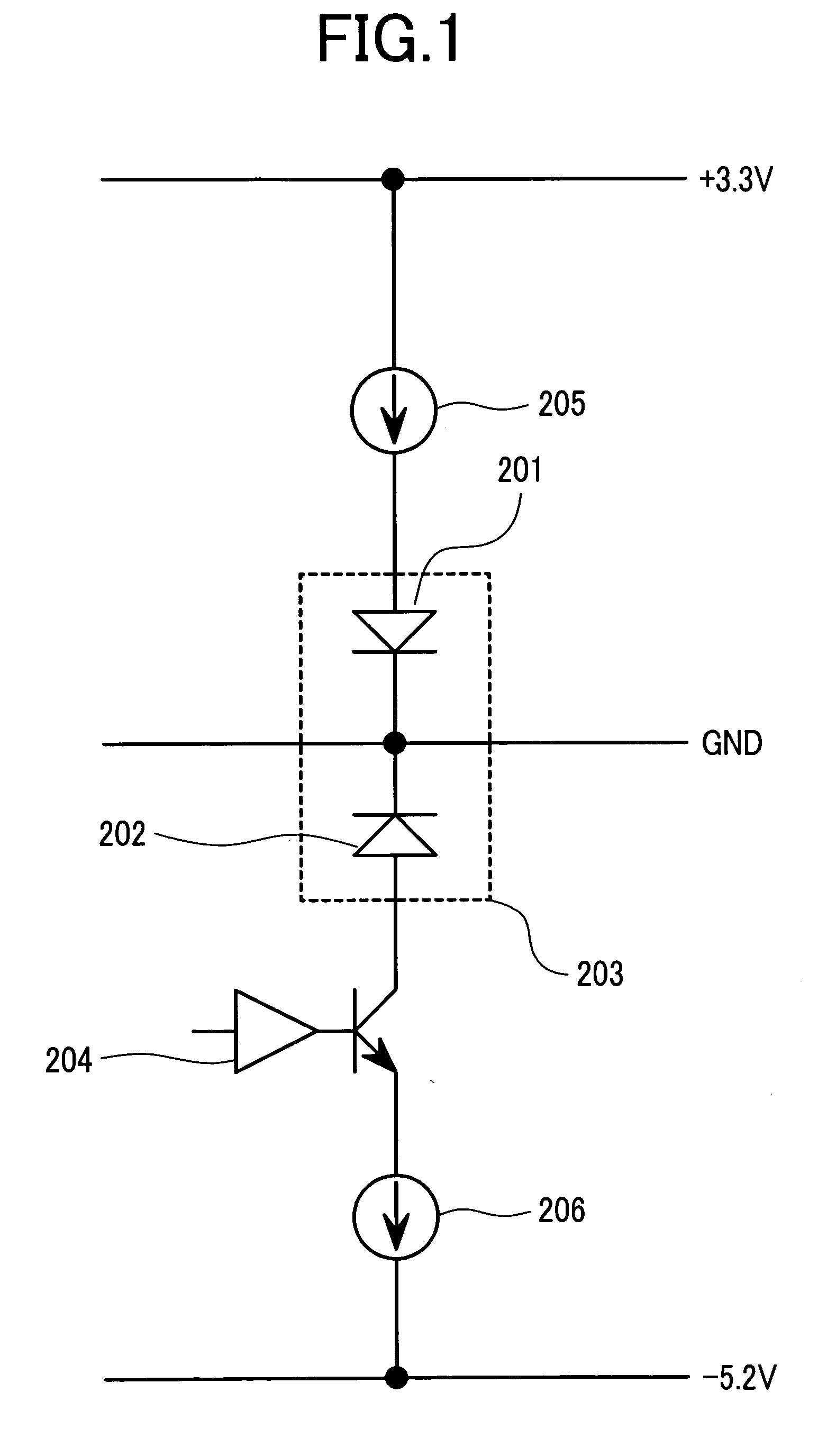
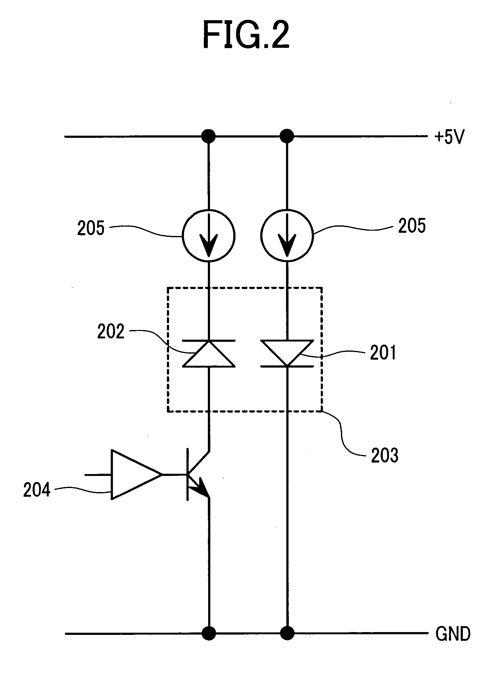
[0049]FIG. 11 is a schematic view of a third embodiment of the present invention. This embodiment is a compact optical transmission module in which an optical modulator-integrated laser is mounted. The optical modulator-integrated laser according to the present invention can be driven by a single power supply. The optical modulator-integrated laser 203 having a DFB laser 210 and an EA modulator 202 integrated monolithically according to the first or second embodiment is mounted in the compact optical transmission module 212. A driver IC 204 for the EA modulator and driver IC 214 for the DFB laser may be integrated on the same chip as well. As mentioned earlier, this module can be driven by a positive power supply 215 alone, spacing saving and power saving are possible in total.
PUM
 Abstract
Description
Claims
Application Information