Wiring substrate, semiconductor device and manufacturing method thereof

a technology of wiring substrate and semiconductor device, which is applied in the direction of conductive pattern formation, sustainable manufacturing/processing, and final product manufacturing, etc., can solve the problems of low throughput, waste of all materials of wiring or film pattern and resist material, and large number of steps of forming wiring or mask pattern, etc., to achieve high yield, high accuracy, and improve yield

Inactive Publication Date: 2005-12-15
SEMICON ENERGY LAB CO LTD
View PDF56 Cites 99 Cited by
  • Summary
  • Abstract
  • Description
  • Claims
  • Application Information

AI Technical Summary

Benefits of technology

[0011] Moreover, it is another object of the present invention to provide a semiconductor device in which cost reduction and throughput improvement are possible due to the small number of steps and reduction of materials and which has a semiconductor element with a minute structure, and further a manufacturing method thereof.
[0016] As the composition remaining on one side or opposite sides of the conductive layer, metal particles are dispersed in organic resin serving as a solvent. Accordingly, the composition is conductive or insulative depending on the density of metal particles. In other words, the composition provided on a side of the conductive layer is conductive when the density of metal particles is high and the contact area of particles is large. On the other hand, when the density of metal particles is low and the periphery of metal particles is coated with organic resin, the composition remaining on one side or opposite sides of the conductive layer is insulative. Thus, when the composition remaining on one side or opposite sides of the conductive layer is insulative, only the conductive layer irradiated with laser light serves as a wiring or an electrode. Therefore, a stable conductive layer that is resistant to falling down can be formed even when the conductive layer whose aspect ratio is large (longitudinal length>lateral length) is adopted. The coverage of an insulating layer or a semiconductor layer to be formed later can be improved and thus, a highly reliable semiconductor element can be formed.
[0029] According to the present invention, a portion of a composition including metal particles and organic resin is directly irradiated with a laser beam to bake the metal particles, thereby forming a wiring having a minute and narrow width without using a photo mask. In addition, the width of the laser beam is made narrow and a part of the composition is irradiated with the laser beam; therefore, micro fabrication of a film-pattern formed by a droplet-discharging method is possible and a semiconductor element having a minute structure can be formed. Moreover, a semiconductor element having a short channel length can be formed by using the conductive layer as a gate electrode. Therefore, a semiconductor device in which a semiconductor element that operates at high speed is integrated with high density can be formed.
[0031] When a droplet discharging method is employed in forming a film pattern, a droplet can be discharged onto an arbitrary position by changing a relative position of a nozzle that is a discharge opening of a droplet including its film material and a substrate. In addition, a thickness and a width of a pattern to be formed can be adjusted depending on a nozzle diameter, the amount of droplets to be discharged, and a relative relationship between movement speed of a nozzle and that of a substrate to be provided with a discharged droplet. Accordingly, a film pattern can be formed in a desired portion with high accuracy by discharging even over a large substrate having a side of 1 m to 2 m or more. Yield can be improved because misalignment with an adjacent film pattern is not caused. As a result, a semiconductor device can be manufactured with the small number of steps and with high yield.
[0032] Moreover, a liquid crystal television and an EL television having a semiconductor device that is formed according to the above described manufacturing steps can be manufactured at low cost with high throughput and yield.

Problems solved by technology

However, when forming a wiring or a film-pattern using a conventional photolithography process, almost all materials of the wiring or the film pattern and a resist material become wasted and the number of steps of forming the wiring or a mask pattern becomes large; therefore throughput is decreased.
A light-exposure apparatus used in the photolithography process has difficulty in exposing a large substrate to light at once.
Accordingly, a manufacturing method of a semiconductor device using a large substrate needs a plurality of times of light-exposure, which leads to misalignment with an adjacent pattern and reduction in yield.
However, in this case, the tip of the discharge opening is clogged with the material solution because a composition of the material solution is attached thereto, dried or solidified therein, and thus it is difficult to discharge a constant amount of material solution continuously or stably.
Consequently, there is a problem in that throughput or yield of a semiconductor device using the semiconductor element is reduced.

Method used


Image

  • Wiring substrate, semiconductor device and manufacturing method thereof
  • Wiring substrate, semiconductor device and manufacturing method thereof
  • Wiring substrate, semiconductor device and manufacturing method thereof

Examples


embodiment mode 1

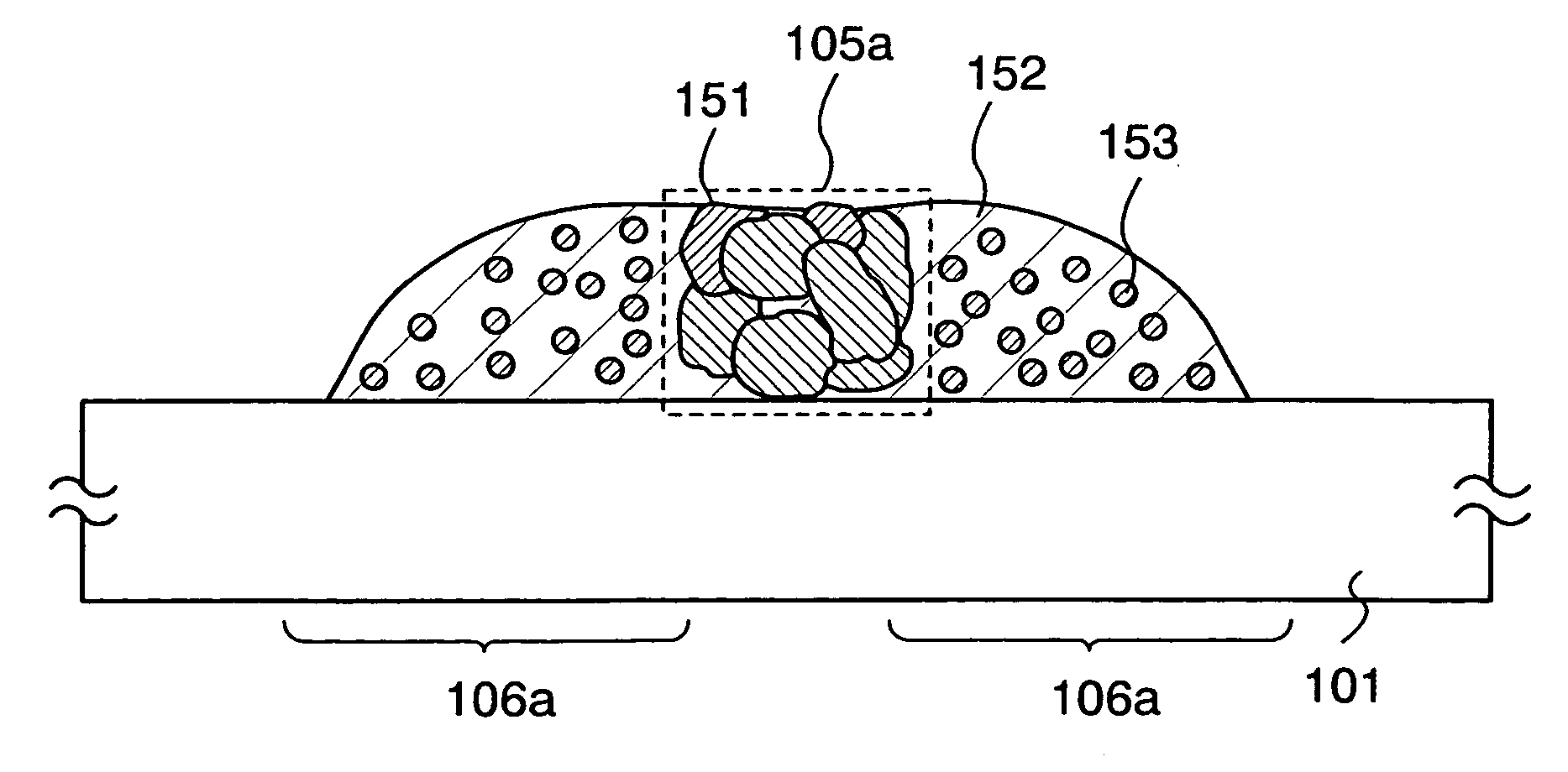
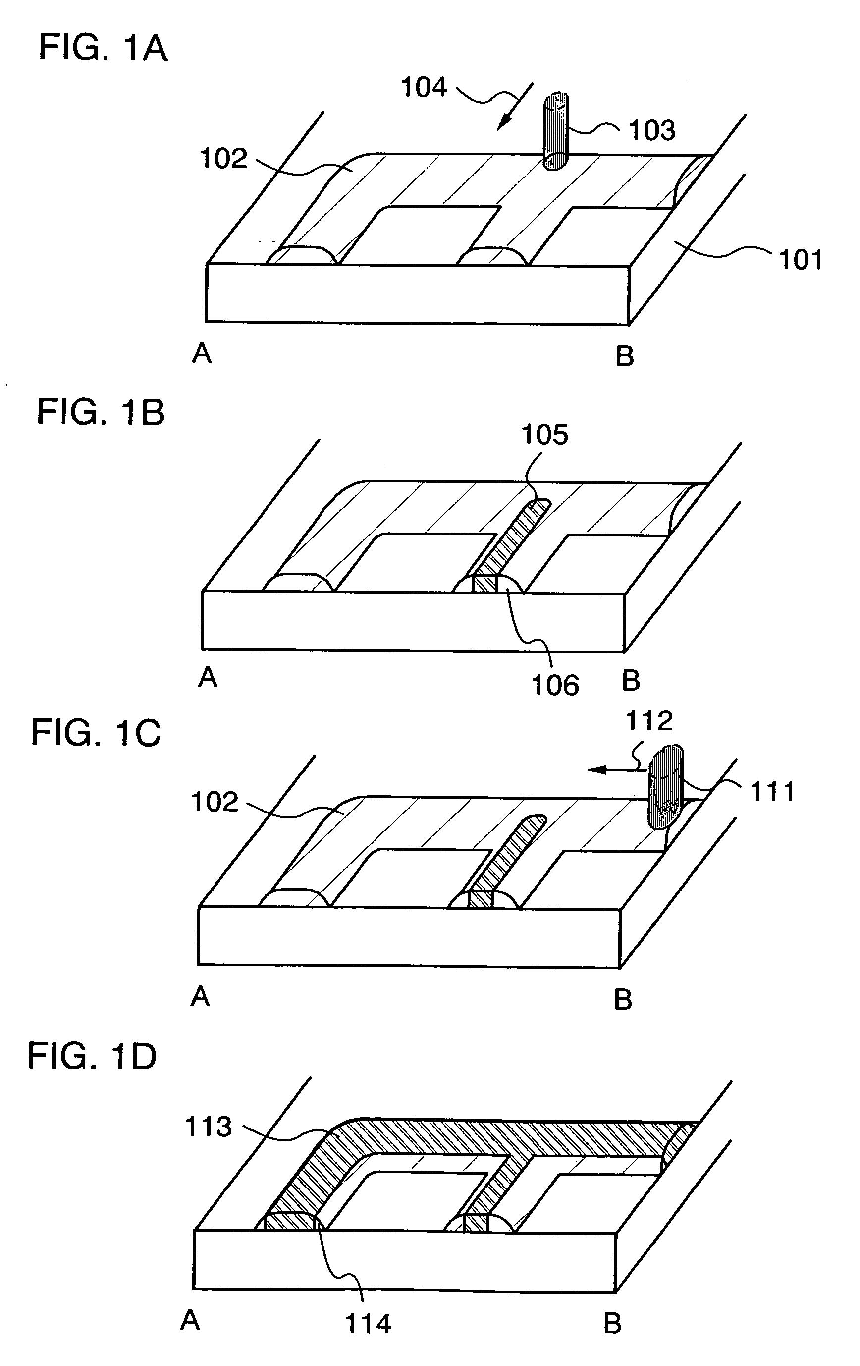
[0067] In Embodiment Mode 1, a process for forming a wiring having a thin width by irradiation of a laser beam (hereinafter referred to as laser light) is described with reference to FIGS. 1A to 1D, 2 and 3A to 3C.

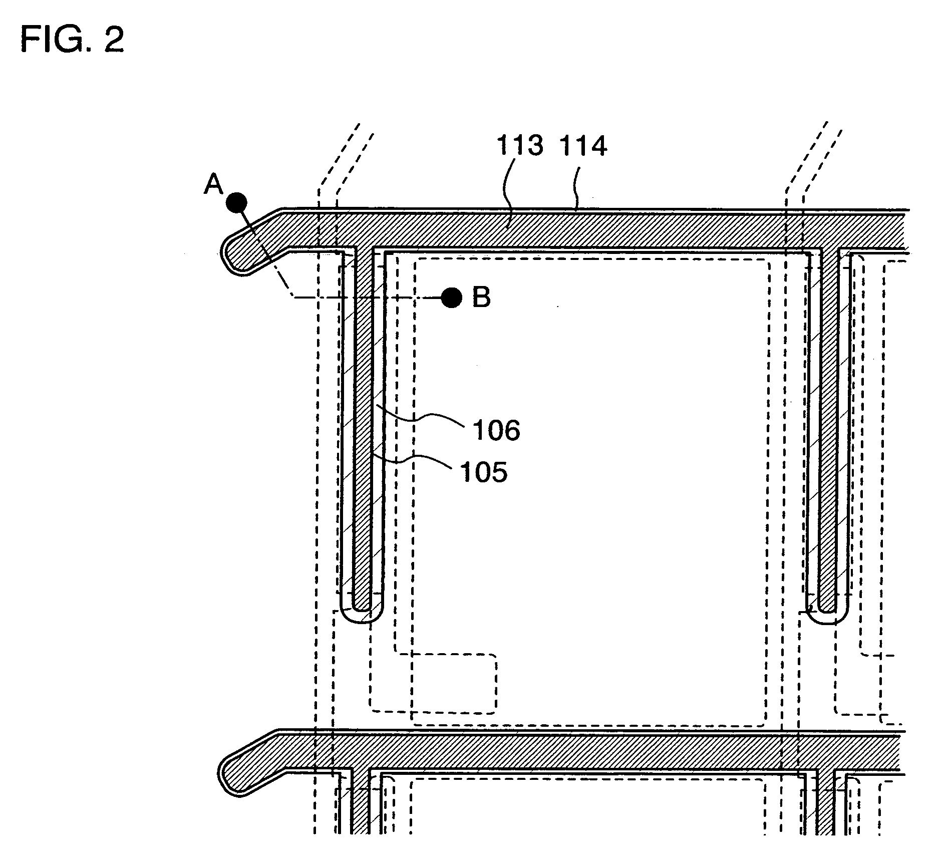
[0068]FIG. 2 is a top view of a substrate 101 in which pixels are arranged in matrix. On the substrate 101, a second conductive layer 113 serving as a gate wiring of a semiconductor element that is to be formed later and a first conductive layer 105 serving as a gate electrode to be connected thereto are shown by a solid line. Note that a dashed line shows a source wiring, a semiconductor region, a source electrode, a drain electrode, a pixel electrode and the like of the semiconductor element that is to be formed later.

[0069]FIGS. 1A to 1D are each a perspective view of a cross-section taken along A-B in FIG. 2. As shown in FIG. 1A, a first pattern material is discharged on the substrate 101 by a droplet discharging method and dried to form a first pattern 102. Note tha...

embodiment mode 2

[0096] Embodiment Mode 2 describes a manufacturing method of a semiconductor element with reference to FIGS. 4A to 4F. In this embodiment mode, a channel etch type TFT of a bottom gate TFT as a semiconductor element is described.

[0097] As shown in FIG. 4A, a first pattern 202 is formed on a substrate 201 by a droplet discharging method. The material of the first pattern 102 shown in Embodiment Mode 1 can be used appropriately for the material of the first pattern 202.

[0098] In this embodiment mode, the first pattern 202 is formed by selectively discharging Ag paste dispersed with silver particles of several nm.

[0099] Then, a part of the first pattern 202 is irradiated with laser light 203 using a laser beam directly-drawing apparatus to form a first conductive layer 211 as shown in FIG. 4B. At this time, in a region that is not irradiated with the laser light 203, the Ag paste remains. Hereinafter, the region where the Ag paste remains is shown as an organic resin layer 212 dispe...

embodiment mode 3

[0116] Embodiment Mode 3 describes a channel protective type TFT of a bottom gate TFT as a semiconductor element with reference to FIGS. 5A to 5F.

[0117] As shown in FIG. 5A, a first conductive layer 211 serving as a gate electrode and an organic resin layer 212 dispersed with metal particles, which is formed on the opposite sides of the first conductive layer 211 are formed on a substrate 201 according to the same steps as in Embodiment Mode 2. After that, a first insulating layer 221 to serve as a gate insulating film and a first semiconductor film 222 are formed. Then, a protective film 301 is formed in a region that exists over the first semiconductor film 222 and overlaps the first conductive layer 211. The formation method and material of the protective film 301 can be similar to those of the first mask pattern 224 shown in Embodiment Mode 2.

[0118] As shown in FIG. 5B, a second semiconductor film (a conductive semiconductor film) 302 is formed. The second semiconductor film 3...


PUM

PropertyMeasurementUnit
widthaaaaaaaaaa
widthaaaaaaaaaa
widthaaaaaaaaaa

Abstract

The present invention provides a method for forming a wiring having a minute shape on a large substrate with a small number of steps, and further a wiring substrate formed by the method. Moreover, the present invention provides a semiconductor device in which cost reduction and throughput improvement are possible due to the small number of steps and reduction of materials and which has a semiconductor element with a minute structure, and further a manufacturing method thereof. According to the present invention, a composition including metal particles and organic resin is irradiated with laser light and a part of the metal particles is baked to form a conductive layer typified by a wiring, an electrode or the like over a substrate. Further, a semiconductor device having the baked conductive layer as a wiring or an electrode is formed.

Description

BACKGROUND OF THE PRESENT INVENTION [0001] 1. Field of the Present Invention [0002] The present invention relates to a wiring substrate and a semiconductor device having a semiconductor element formed by a droplet discharging method typified by an ink-jet method, and further manufacturing methods thereof. [0003] 2. Description of the Related Art [0004] Conventionally, an active matrix driving type display panel or semiconductor integrated circuit including a semiconductor element typified by a thin film transistor (hereinafter, TFT) or a MOS transistor is formed by patterning each thin film with light-exposure process (hereinafter, a photolithography process) using a photomask. [0005] In the photolithography process, resist is applied to a whole substrate, pre-baked, then the substrate is irradiated with ultraviolet rays or the like using a photomask and a resist pattern is formed by development. After that, a thin film existing outside a portion to be a film pattern or a wiring (a ...

Claims


Application Information

Patent Timeline
Patent Type & Authority Applications(United States)
IPC IPC(8): B05D3/00B05D5/12B29C71/02B32B3/00H01L21/28H01L21/288H01L21/336H01L21/768H01L21/77H01L29/45H05K1/09H05K3/12
CPCH01L21/28008H01L21/28026H01L2924/1305Y10T428/24917H01L2924/07811H01L21/28079H01L21/28123H01L21/288H01L21/76823H01L21/76825H01L21/76838H01L21/76894H01L29/458H01L29/4908H01L29/66757H01L29/66765H05K1/095H05K3/1283H05K2201/0215H05K2203/0597H05K2203/107H05K2203/1131H01L27/1292H01L2924/13091H01L2224/4847H01L2924/00H01L2924/12044Y02P70/50
Inventor YAMAMOTO, HIROKONAKAMURA, OSAMU
Owner SEMICON ENERGY LAB CO LTD
Why Eureka
Try Eureka