Method of identifying logical information in a programming and erasing cell by on-side reading scheme

a logical information and programming technology, applied in the field of one-side reading scheme for identifying logical information in a programming and erasing cell, can solve the problems of high power consumption, complex manufacturing process of flash eeprom, and large production cost of the product, and achieve the effect of improving the local dibl

Active Publication Date: 2005-12-29
MACRONIX INT CO LTD
View PDF3 Cites 11 Cited by
  • Summary
  • Abstract
  • Description
  • Claims
  • Application Information

AI Technical Summary

Benefits of technology

[0016] It is therefore an object of the invention to provide a method of identifying logical information in a programming and erasing cell, particularly in a programming by hot hole injection nitride electron storage (PHINES) cell, by one-side reading scheme, thereby easing the limitation of 2nd-bit effect and hole-enhance local-DIBL effect, and controlling the operation window.

Problems solved by technology

However, the manufacturing process of flash EEPROM is complicated and the production cost thereof is very expansive.
However, the NROM device has the problems such as high power consumption due to hot electron programming and read disturbance, which are potential issues for scaling ability.
However, reading the PHINES cell in the reverse direction has the drawbacks, such as 2nd-bit effect (higher Vread applied for reading in the reverse direction) thereby limiting the sensing window and the scaling ability, and hole-enhance local-DIBL (drain induced barrier lowing) effect (FIG. 4).

Method used


Image

  • Method of identifying logical information in a programming and erasing cell by on-side reading scheme
  • Method of identifying logical information in a programming and erasing cell by on-side reading scheme
  • Method of identifying logical information in a programming and erasing cell by on-side reading scheme

Examples


first embodiment

[0034]FIG. 5A˜FIG. 5D schematically show the state of erasing, programming and reading the PHINES cell and the related logical information of two bits according to the invention. Please also refer FIG. 1 for the structure of a PHINES cell.

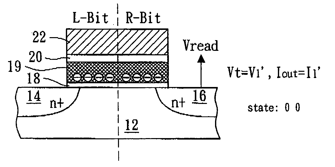
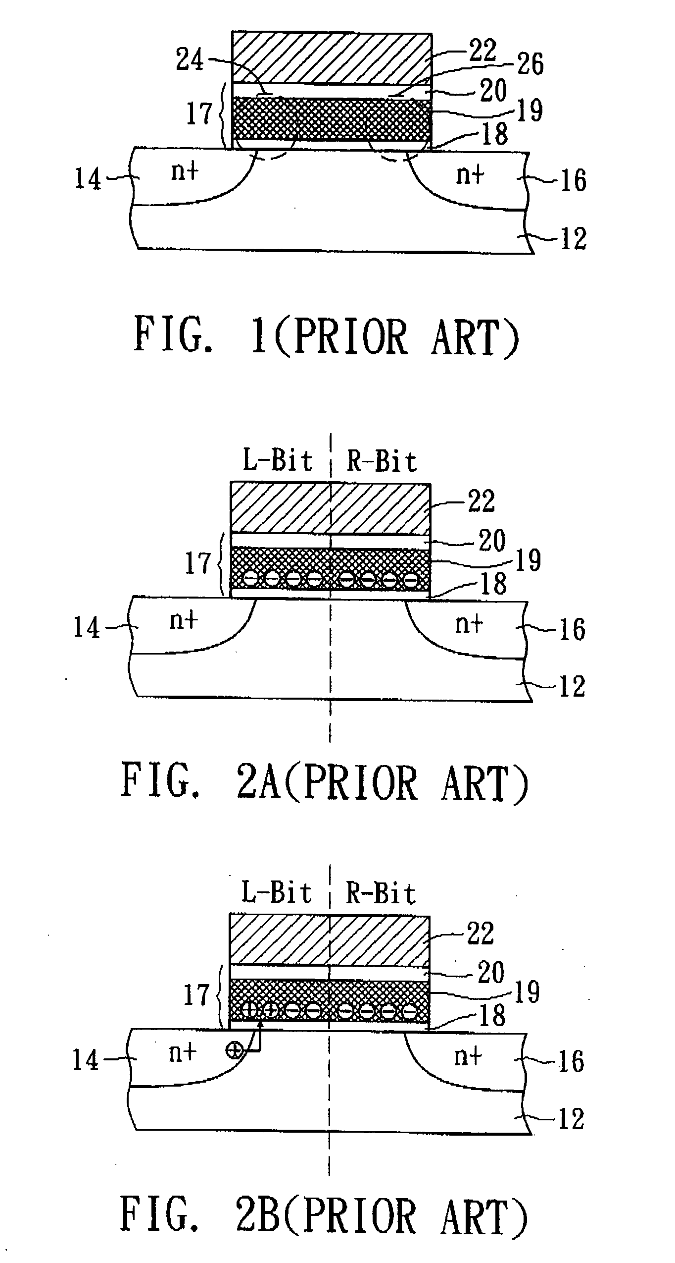
[0035] The PHINES cell comprises a substrate 12 (typically a P-type substrate), a source 14 and a drain 16 separated by the channel, and two buried PN junctions. The left PN junction is between the source 14 and the substrate 12, and the right PN junction is between the drain 16 and the substrate 12. Above the channel is an oxide-nitride-oxide (ONO) stack 17, comprising a silicon dioxide layer 18, a silicon nitrite layer 19 and a silicon dioxide layer 20. Also, a control gate 22 is formed over the ONO stack 17. The silicon dioxide layer 18 forms as an electrical isolation layer over the channel. The silicon nitrite layer 19 functions as a trapping storage layer. The silicon dioxide layer 20 electrically isolates the silicon nitride layer 19 and the...

second embodiment

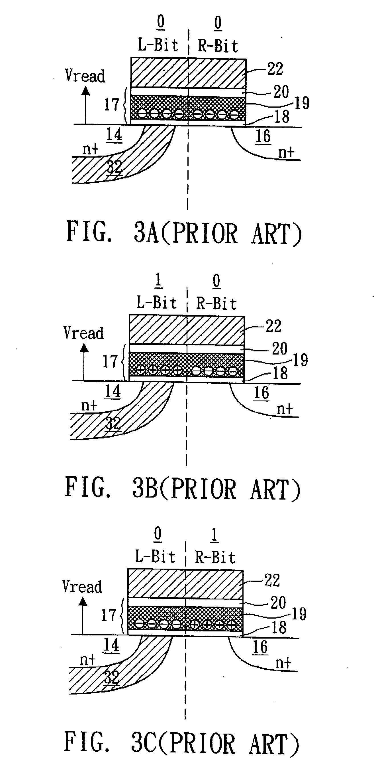
[0039]FIG. 8A˜FIG. 8D schematically show the state of erasing, programming and reading the PHINES cell and the related logical information of two bits according to the invention. It is also assumed that a read voltage is applied to the drain 16 for reading the logical information of the PHINES cell.

[0040] In FIG. 8A, the L-Bit and the R-Bit of the PHINES cell are erased before proceeding the programming step. During the erasing step, the threshold voltage (Vt) is increased with the erasing time, and the tendency of the curve (Vt vs. erasing time) is similar as the curve represented in FIG. 6. After erase of the L-Bit and the R-Bit is completed, Vt is increased to the certain value V1.

[0041] In FIG. 8B˜8D, the L-Bit and the R-Bit are programmed by hot hole injection. The Vt is decreased with the programming time.

[0042] As shown in FIG. 8B, two hot holes are injected to the silicon nitride layer 19 of the L-Bit and the R-Bit, respectively. The threshold voltage (Vt) is V2′ and the o...


PUM


Abstract

A method of identifying logical information in a cell, particularly in a programming by hot hole injection nitride electron storage (PHINES) cell by one-side reading scheme is disclosed. The method comprise steps of: erasing the first region and the second region of PHINES cell by increasing a local threshold voltage (Vt) to a certain value; programming at least one of the first region and the second region of the PHINES cell by hot hole injection; and reading a logical state of the PHINES cell by measuring an output current of one of the first region and the second region; wherein different quantity of the output current is caused by interaction between different quantity of the hot hole stored in the first region and the second region, so as to determine the logical state of the PHINES cell by one-side reading scheme.

Description

BACKGROUND OF THE INVENTION [0001] 1. Field of the Invention [0002] The invention relates in general to a method of identifying logical information in a programming and erasing cell by one-side reading scheme, and more particularly to the method of identifying logical information in a programming by hot hole injection nitride electron storage (PHINES) cell by one-side reading scheme. [0003] 2. Description of the Related Art [0004] Semiconductor device, having the advantages that the information stored therein is not lost even the power supply is removed, so labeled as “non-volatile memory” is current widespread use today. The non-volatile semiconductor memory, such as read only memory (ROM), programmable read only memory (PROM), erasable programmable read only memory (EPROM), electrical erasable programmable read only memory (EEPROM) and flash EEPROM, are used in various application. [0005] Semiconductor EEPROM device involves more complicate processing and testing procedures than o...

Claims


Application Information

Patent Timeline
Patent Type & Authority Applications(United States)
IPC IPC(8): G11C16/04H01L21/8247
CPCG11C16/0475
Inventor WU, CHAO-ILEE, MING-HSIUHSU, TZU-HSUAN
Owner MACRONIX INT CO LTD
Why Eureka
Try Eureka