Semiconductor device and Manufacturing method thereof

a semiconductor device and semiconductor technology, applied in the direction of semiconductor devices, basic electric elements, electrical appliances, etc., can solve the problems of fear of a failure of the transistor, the inability to read (determine) stored data from the transistor, etc., to prevent a failure of the semiconductor device effectively, enhance yield, and enhance the electrical characteristic of the semiconductor device

Active Publication Date: 2007-10-04
LAPIS SEMICON CO LTD
View PDF7 Cites 6 Cited by
  • Summary
  • Abstract
  • Description
  • Claims
  • Application Information

AI Technical Summary

Benefits of technology

[0022]According to a configuration example of a semiconductor device of the present invention, four respective partial regions of an electron storage layer, which are opposite to four side surfaces of a gate electrode shaped in the form of an approximately quadrangular prism, hold electrons. Therefore, even though the electrons exist in the partial regions on the opposed sides in particular upon operation, the cell current windows already described above are no longer narr

Problems solved by technology

There is a fear that when the cell current windows are varied and narrowed as described above, the reading (determinatio

Method used


Image

  • Semiconductor device and Manufacturing method thereof
  • Semiconductor device and Manufacturing method thereof
  • Semiconductor device and Manufacturing method thereof

Examples


first preferred embodiment

(Configuration Example 1 of Semiconductor Device)

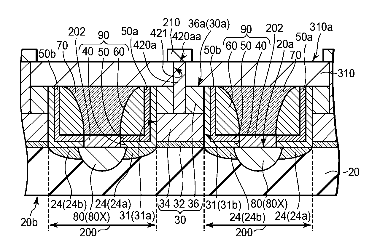
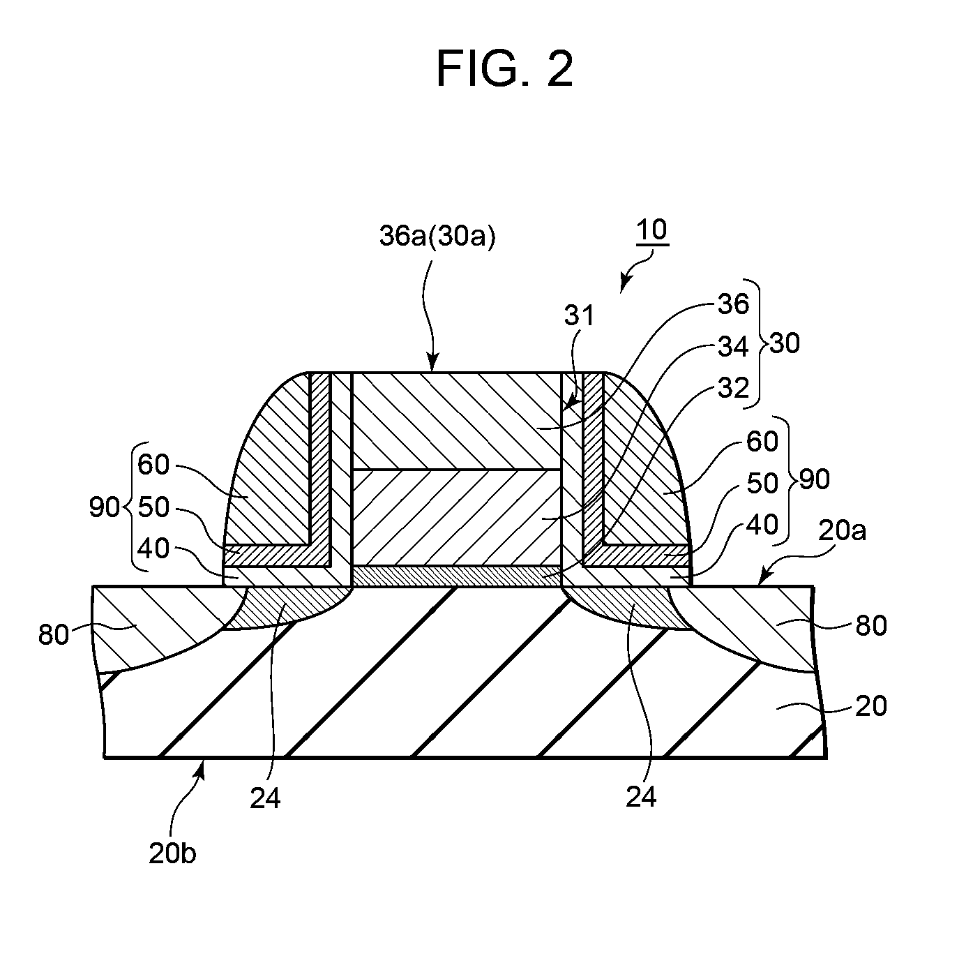
[0053]A configuration example of a semiconductor device (which also means a semiconductor element or chip, i.e., a transistor) of the present invention will be explained with reference to FIGS. 1, 2, 3 and 4. Incidentally, the semiconductor device of the present invention features configurations of a gate electrode and a sidewall.

[0054]FIGS. 1(A) and 1(B) are typical perspective views for describing an overall configuration of the semiconductor device of the present invention. FIG. 1(B) shows part of the semiconductor device in cut-away form to make it easy to understand the configurations of the gate electrode and sidewall.

[0055]FIG. 2 is a typical view showing a cut cross-section cut along one-dot chain line I-I′ shown in FIG. 1(B) or one-dot chain line II-II′ shown in FIG. 1(B).

[0056]FIGS. 3(A) and 3(B) are respectively typical perspective views for describing the configuration of the gate electrode.

[0057]FIG. 4(A) is a typical vie...

example 1

(Example 1 of Semiconductor Device Manufacturing Method)

[0101]An example of a method for manufacturing a semiconductor device of the present invention will be explained with reference to FIGS. 5, 6, 7 and 8.

[0102]FIGS. 5(A), 5(B) and 5(C) are respectively typical manufacturing process views for describing a process for manufacturing the semiconductor device of the present invention. FIG. 5(A) is a plan schematic view of the semiconductor device, FIG. 5(B) is a schematic view showing a cut cross-section cut along one-dot chain line III-III′ of FIG. 5(A), and FIG. 5(C) is a schematic view showing a cut cross-section cut along one-dot chain line IV-IV′ of FIG. 5(A).

[0103]FIGS. 6(A), 6(B) and 6(C) are respectively manufacturing process views following FIG. 5(C), showing cut cross-sections each cut at the same position as one-dot chain line IV-IV′ of FIG. 5(A).

[0104]FIG. 7 is a manufacturing process view following FIG. 6(C).

[0105]FIG. 8(A) is a manufacturing process view following FIG. 7...

second preferred embodiment

[0148](Configuration Example 2 of Semiconductor Device)

[0149]A configuration example of a semiconductor device of the present invention will be explained with reference to FIGS. 9(A) and 9(B). Incidentally, the semiconductor device of the present example has a feature in that the position of a gate electrode is shifted between adjacent sidewalls as compared with the first embodiment already described above.

[0150]FIG. 9(A) is a plan typical view of the semiconductor device as viewed from its upper surface side, and FIG. 9(B) is a typical view illustrating a cut cross-section cut along one-dot chain line V-V′ shown in FIG. 9(A).

[0151]As shown in FIGS. 9(A) and 9(B), the semiconductor device 10 includes a first conduction type substrate 20. In the present example, the first conduction type substrate 20 is of a P type substrate.

[0152]As shown in FIG. 9(B), the first conduction type substrate 20 has a front surface 20a and a back surface 20b opposite to the front surface 20a.

[0153]The s...


PUM


Abstract

The present invention provides a semiconductor device which includes a gate electrode shaped in the form of an approximately quadrangular prism, including a laminated body of a gate oxide layer, a gate polysilicon layer and a gate silicon nitride layer provided in a first conduction type substrate, a second conduction type implantation region provided in a region outside the gate electrode, a sidewall that exposes a top face of the gate electrode and is formed by laminating a sidewall mask oxide layer covering side surfaces, an electron storage nitride layer and a sidewall silicon oxide layer, and a source/drain diffusion layer provided in the first conduction type substrate exposed from the gate electrode and the sidewall.

Description

BACKGROUND OF THE INVENTION[0001]The present invention relates to a semiconductor device and a manufacturing method thereof, and particularly to a transistor element capable of performing 4-bit writing, and a semiconductor device equipped therewith and a manufacturing method thereof.[0002]There has been known, for example, a semiconductor device that implements a ferroelectric memory cell capable of storing polarization data of a multivalue of three values or more in one ferroelectric film.[0003]According to the configuration of the conventional semiconductor device, information equivalent to 4 bits in total are stored at positions of 4 points in total corresponding to two points of both ends as viewed in a first direction, of the ferroelectric element, and two points of both ends as viewed in a second direction orthogonal to the first direction (refer to a patent document 1 (Japanese Unexamined Patent Publication No. 2004-047593)).[0004]With the objective of implementing a semicond...

Claims


Application Information

Patent Timeline
IPC IPC(8): H01L29/94
CPCH01L21/28282H01L27/115H01L29/7923H01L29/4234H01L27/11568H01L29/40117H10B43/30H10B69/00
Inventor YUDA, TAKASHI
Owner LAPIS SEMICON CO LTD
Why Eureka
Try Eureka