[0015] The present invention has been achieved in consideration of such problems and an object of the invention is to provide a magnetic sensing device capable of suppressing occurrence of hysteresis to thereby reduce 1 / f noise, stably sensing a signal magnetic field at high sensitivity, and holding the stability even when a strong external magnetic field that disturbs a free layer is applied, and a method of forming the same.
[0018] In the first and second magnetic sensing devices of the invention constructed as described above, as compared with the case where the magnetization directions of the pinned layer and the free layer are orthogonal to each other when the external magnetic field is zero, variations in the directions of
spins in the magnetic domains in the free layer are reduced. Consequently, when read current is passed in a state where the external magnetic field is applied in the direction orthogonal to the magnetization direction of the pinned layer, occurrence of hysteresis in the relation between a change in the external magnetic field and the resistance change is suppressed, and stability of the free layer also improves. In particular, in the case where the direction of the easy axis of magnetization of the free layer is parallel to the magnetization direction of the pinned layer, the directions of
spins in the magnetic domains are easily aligned and hyseresis is reduced more.
[0022] In the methods of forming the first and second magnetic sensing devices according to the invention, the setting of the magnetization directions of the first and second ferromagnetic
layers in the initial state where the external magnetic field is zero is completed by the regularization step. Consequently, as compared with the case where the first and second ferromagnetic
layers have the magnetization directions which are orthogonal to each other, variations in the directions of
spins in the magnetic domains in the first ferromagnetic layer are reduced. Therefore, the magnetic sensing device is obtained such that when read current is passed in a state where the external magnetic field is applied in the direction orthogonal to the magnetization direction of the second ferromagnetic layer, occurrence of hysteresis in the relation between a change in the external magnetic field and the resistance change is suppressed and stability of the free layer improves.
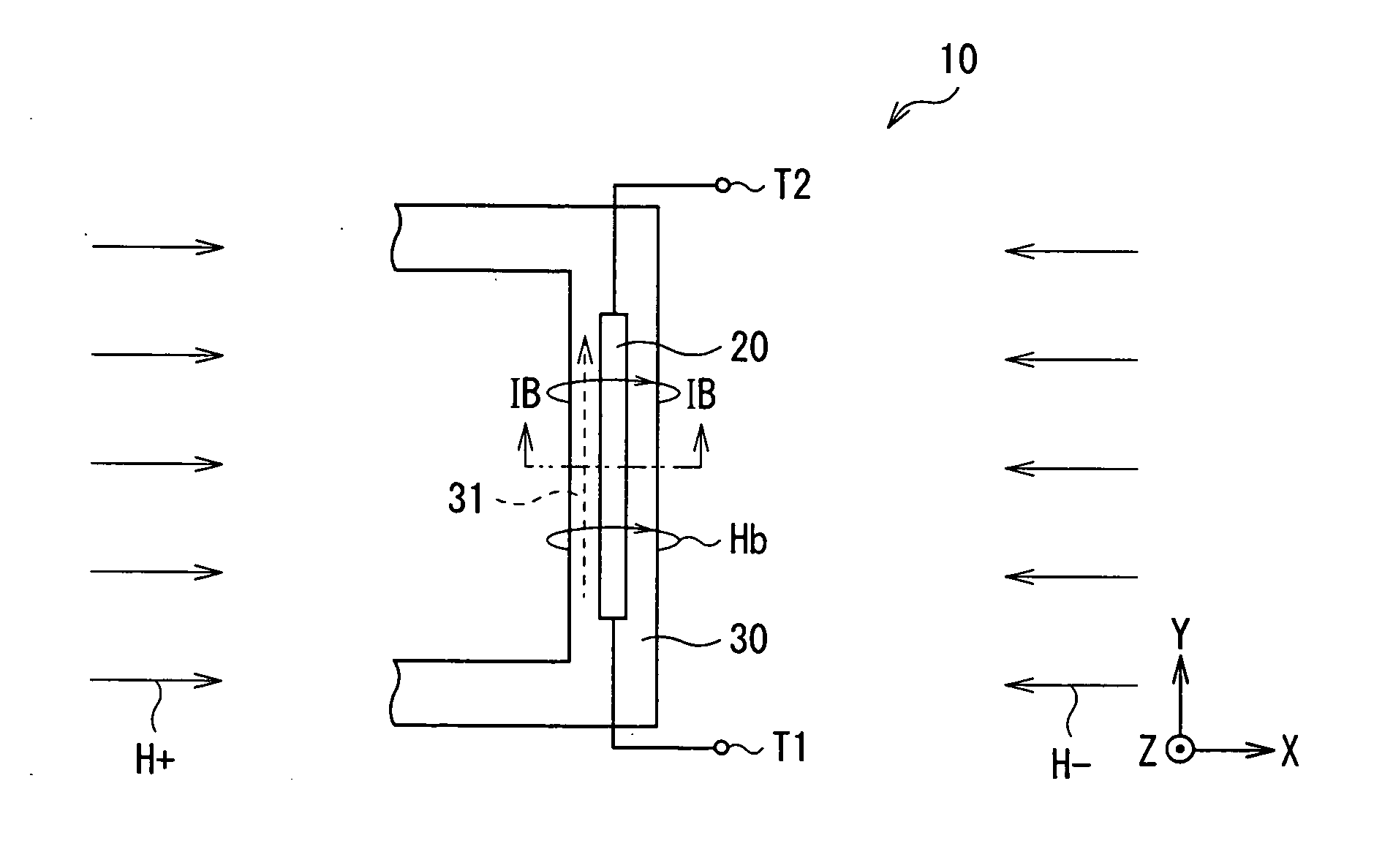
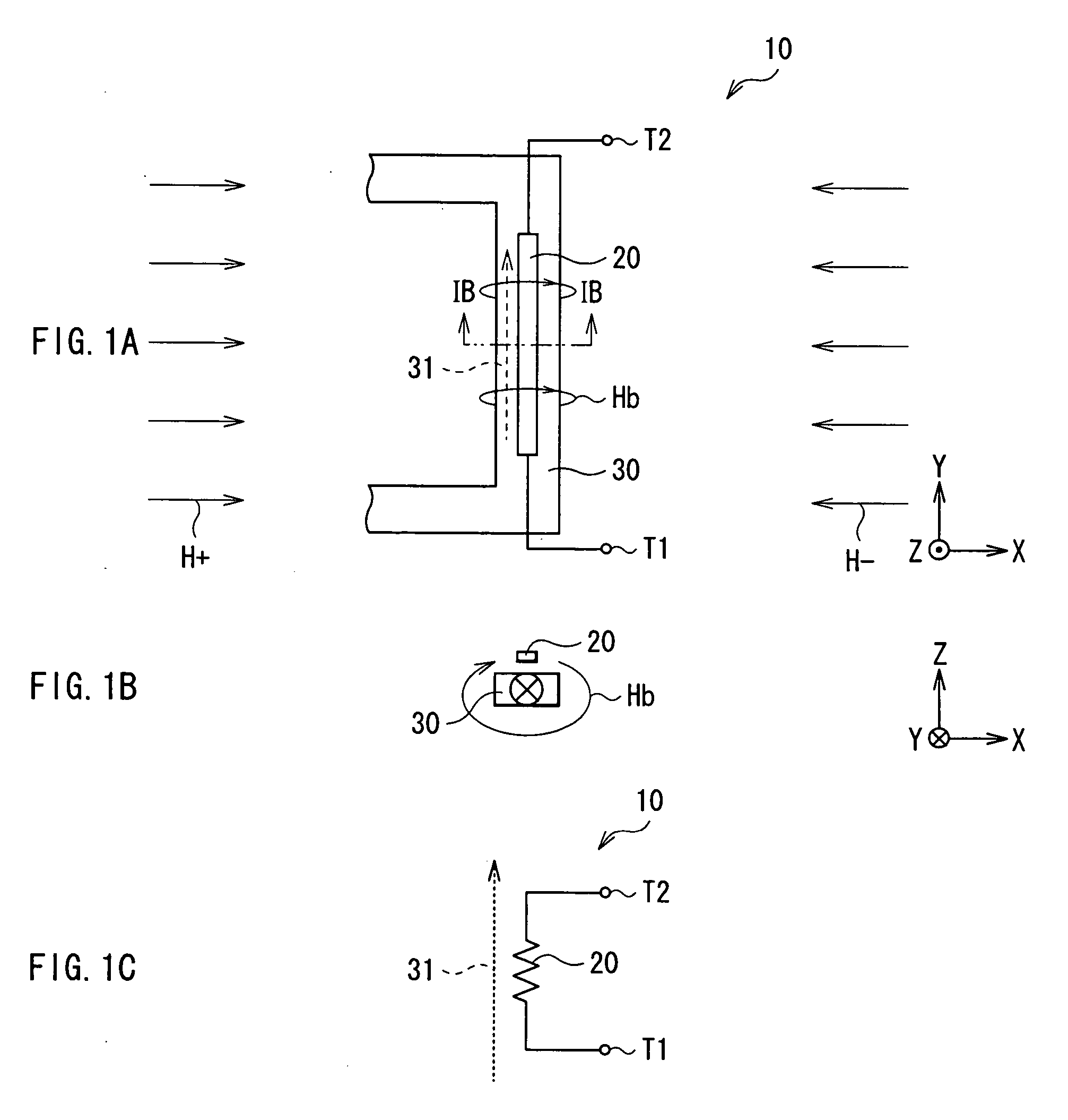
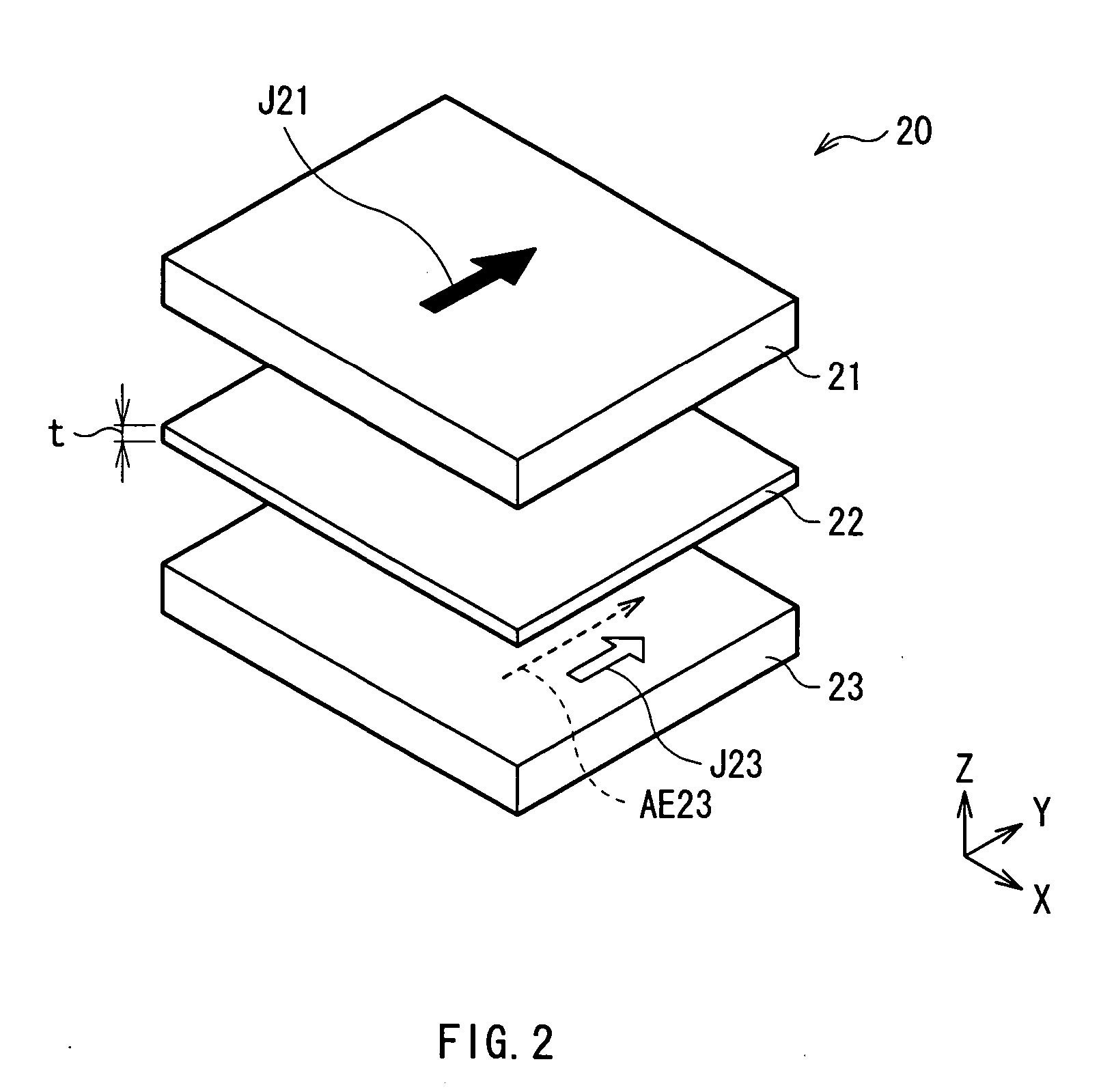
[0027] The first magnetic sensing device of the invention has a stacked body including: a pinned layer having a magnetization direction pinned in a predetermined direction; a free layer whose magnetization direction changes according to an external magnetic field and, when the external magnetic field is zero, becomes parallel to the magnetization direction of the pinned layer; and an intermediate layer sandwiched between the pinned layer and the free layer. The intermediate layer has a thickness at which an
exchange bias magnetic field in the magnetization direction of the pinned layer becomes positive. The
exchange bias magnetic field is generated between the pinned layer and the free layer. Therefore, in the case of passing read current in a state where the external magnetic field is applied in the direction orthogonal to the magnetization direction of the pinned layer, occurrence of hysteresis in the relation between a change in the external magnetic field and the resistance change can be suppressed, and stability of the free layer also improves. Moreover, different from the case of using shape
anisotropy, deterioration in sensitivity does not occur. As a result, 1 / f noise is suppressed and a signal magnetic field can be stably sensed at high sensitivity. In particular, the value of the magnetic
field intensity can be measured accurately and continuously, so that the invention can be sufficiently applied not only to a digital sensor but also to an analog sensor. In particular, when the free layer has the easy axis of magnetization parallel to the magnetization direction of the pinned layer, variations in the directions of spins in the free layer can be reduced. As a result, sensitivity and stability can be further improved.
[0030] The method of forming the first magnetic sensing device of the invention includes: a stacking step of forming a stacked body by sequentially forming a first ferromagnetic layer whose magnetization direction changes according to an external magnetic field, an intermediate layer, and a second ferromagnetic layer having coercive force larger than that of the first ferromagnetic layer; and a regularization step of making a regularization so that the magnetization directions of the first and second ferromagnetic
layers become parallel to each other. The intermediate layer is formed so as to have a thickness at which an exchange bias magnetic field in the magnetization direction of the second ferromagnetic layer becomes positive, the exchange bias magnetic field is generated between the first and second ferromagnetic layers, and setting of the magnetization directions of the first and second ferromagnetic layers in an initial state where the external magnetic field is zero is completed by the regularization step. Consequently, the magnetic sensing device can be obtained in which, in the case of passing read current in a state where the external magnetic field is applied in the direction orthogonal to the magnetization direction of the pinned layer, occurrence of hysteresis in the relation between a change in the external magnetic field and the resistance change can be suppressed, and stability of the free layer also improves. Moreover, different from the case of using shape
anisotropy, deterioration in sensitivity does not occur. In particular, by forming the first ferromagnetic layer so as to have the easy axis of magnetization, making the regularization by performing the annealing process while applying the magnetic field in the same direction as the direction of the easy axis of magnetization, and setting the magnetization directions of the first and second ferromagnetic layers to be parallel to the easy axis of magnetization, variations in the spin directions can be further reduced. As a result, 1 / f noise is suppressed and a signal magnetic field can be stably sensed at high sensitivity. In this case, the value of the magnetic
field intensity itself can be measured accurately and continuously, so that the invention can be sufficiently applied not only to a digital sensor but also to an analog sensor. In particular, when the free layer has the easy axis of magnetization parallel to the magnetization direction of the pinned layer, variations in the directions of spins in the free layer can be reduced. As a result, sensitivity and stability can be further improved.
[0031] The method of forming the second magnetic sensing device of the invention includes: a stacking step of forming a stacked body by sequentially forming a first ferromagnetic layer whose magnetization direction changes according to an external magnetic field, an intermediate layer, and a second ferromagnetic layer having coercive force larger than that of the first ferromagnetic layer; and a regularization step of making a regularization so that the magnetization directions of the first and second ferromagnetic layers become anti-parallel to each other. The intermediate layer is formed so as to have a thickness at which an exchange bias magnetic field in the magnetization direction of the second ferromagnetic layer becomes negative, the exchange bias magnetic field is generated between the first and second ferromagnetic layers, and setting of the magnetization directions of the first and second ferromagnetic layers in an initial state where the external magnetic field is zero is completed by the regularization step. Consequently, the magnetic sensing device can be obtained in which, in the case of passing read current in a state where the external magnetic field is applied in the direction orthogonal to the magnetization direction of the pinned layer, occurrence of hysteresis in the relation between a change in the external magnetic field and the resistance change can be suppressed, and stability of the free layer also improves. Moreover, different from the case of using shape
anisotropy, deterioration in sensitivity does not occur. In particular, when the regularization is made by sequentially performing the first step of performing the annealing process while applying the magnetic field in the same direction as the direction of the easy axis of magnetization of the first ferromagnetic layer, the second step of performing the annealing process while applying the magnetic field in the direction opposite to the direction of the easy axis of magnetization, and the third step of performing the annealing process while applying the magnetic field in the same direction as that of the easy axis of magnetization, the magnetization direction of the second ferromagnetic layer is set to be parallel to the easy axis of magnetization, and the magnetization direction of the first ferromagnetic layer is set to be anti-parallel to the easy axis of magnetization, variations in the spin directions can be further reduced. Therefore, effects similar to those of the method of forming the first magnetic sensing device of the invention can be obtained.

