Method of growing semi-insulating GaN layer

a technology of undoped gan and semi-insulating gan, which is applied in the direction of basic electric elements, electrical apparatus, semiconductor devices, etc., can solve the problems of many defects, high production cost, and difficult growth of single crystals, and achieve high sheet resistance

Inactive Publication Date: 2006-01-05
SAMSUNG ELECTRO MECHANICS CO LTD
View PDF2 Cites 31 Cited by
  • Summary
  • Abstract
  • Description
  • Claims
  • Application Information

AI Technical Summary

Benefits of technology

[0011] Therefore, the present invention has been made in view of the above problems of the prior art, and it is an object of the present invention to provide a method for growing a semi-insulating GaN layer with high sheet resistance by controlling the size of grains through changes in growth temperature at the initial growth stage of the layer, without doping of dopants such as Zn, Mg, C, Fe, etc.

Problems solved by technology

However, since there is a large difference in the lattice constant and thermal expansion coefficient between the sapphire substrate and the GaN layer, the growth of a single crystal is difficult and many defects are generated during growth of the layer.
In addition, nitrogen vacancies are formed due to highly volatile nitrogen.
Furthermore, since n-type conductivity naturally takes place due to the influence of impurities, such as oxygen, it is difficult to form a semi-insulating layer.
For these reasons, a leakage current is caused during fabrication of electronic devices, such as HFETs and SAW devices, leading to low transconductance and increased insertion loss.
However, the dopants may remain in a chamber where the GaN layer is grown, resulting in doping into unwanted layers, i.e., memory effect.
This conductive GaN layer cannot ensure sufficient insulation between devices, causing malfunction of the devices.
Further, doping of high-concentration dopants leads to degraded crystallinity and adversely affects the performance of the devices.

Method used


Image

  • Method of growing semi-insulating GaN layer
  • Method of growing semi-insulating GaN layer
  • Method of growing semi-insulating GaN layer

Examples


Embodiment Construction

[0028] A method for growing a semi-insulating GaN layer according to the present invention will now be described in more detail with reference to the accompanying drawings.

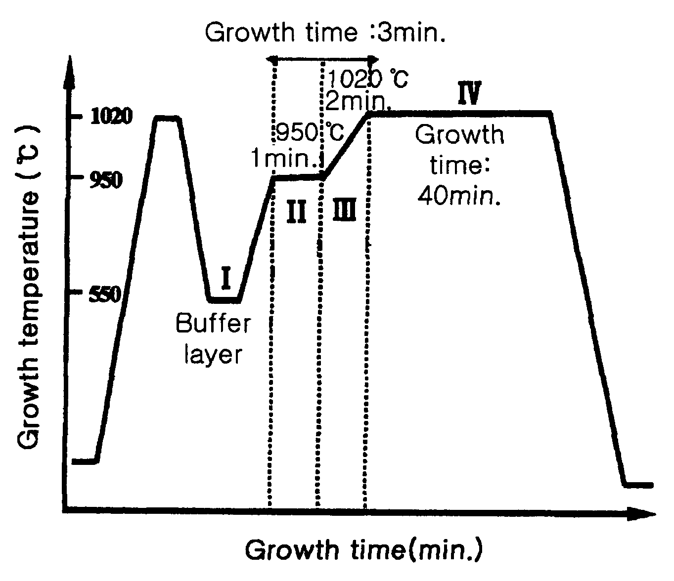
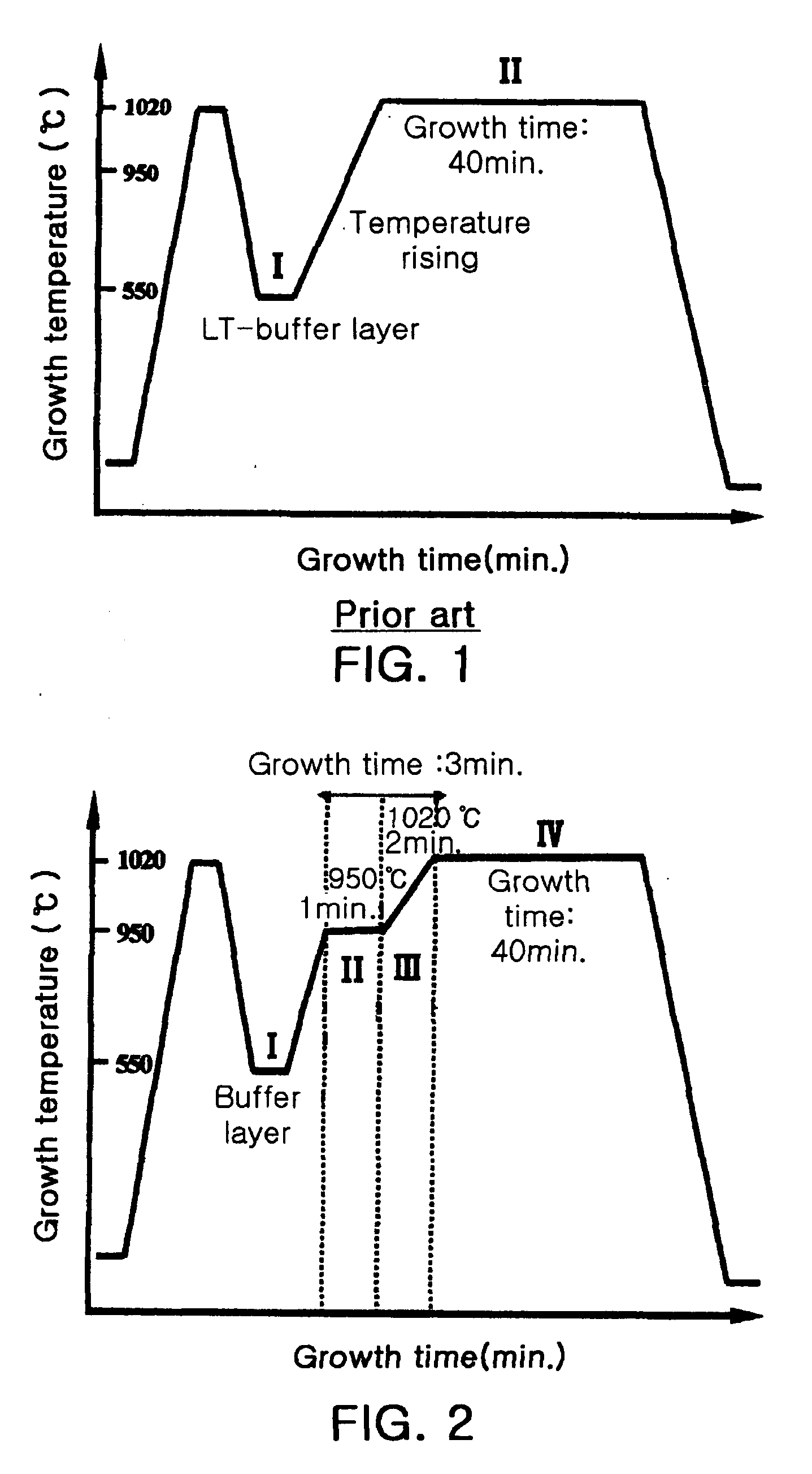
[0029]FIG. 2 is a growth time-growth temperature graph showing the procedure of a method for growing a semi-insulating GaN layer according to the present invention. Referring to FIG. 2, a buffer layer is grown on a sapphire substrate at a first growth temperature (I). Since there is no substrate having a lattice constant and a thermal expansion coefficient identical to those of GaN as a nitride semiconductor material, it is common that a buffer layer is previously grown on a sapphire substrate. In order to reduce the difference in the lattice constant and thermal expansion coefficient between the sapphire substrate and a nitride semiconductor material to be grown thereon, and to prevent the degradation of crystallinity, the buffer layer is preferably formed to a small thickness at low temperature. The buffer laye...


PUM


Abstract

Disclosed herein is a method for growing a semi-insulating GaN layer with high sheet resistance by controlling the size of grains through changes in growth temperature at the initial growth stage of the layer, without doping of dopants. The method comprises the steps of growing a buffer layer on a substrate at a first growth temperature, growing a GaN layer on the buffer layer at a second growth temperature higher than the first growth temperature for a first growth time (a first growth step), growing the GaN layer at increasing temperatures from the second growth temperature to a third growth temperature higher than the second growth temperature for a second growth time (a second growth step), and growing the GaN layer at the third growth temperature for a third growth time (a third growth step).

Description

RELATED APPLICATIONS [0001] The present application is based on, and claims priority from, Korean Application Number 2004-51983, filed Jul. 5, 2004, the disclosure of which is hereby incorporated by reference herein in the entirety. BACKGROUND OF THE INVENTION [0002] 1. Field of the Invention [0003] The present invention relates to a method for growing a semi-insulating undoped GaN layer, and more particularly to a method for growing an undoped GaN layer with high sheet resistance by controlling the size of grains through changes in growth temperature at the initial growth stage of the layer, without doping of dopants. [0004] 2. Description of the Related Art [0005] With the recent development of digital communication technologies, communication technologies for ultrahigh-speed and high-capacity signal transmission have been rapidly advanced. In particular, as the demands on personal cellular phones, satellite communications, military radars, broadcasting communications, communicati...

Claims


Application Information

Patent Timeline
Patent Type & Authority Applications(United States)
IPC IPC(8): H01L21/20
CPCH01L21/0242H01L21/02458H01L21/0262H01L21/0254H01L21/02494H01L21/02496H01L21/324H01L2924/1033
Inventor LEE, JAE HOONLEE, JUNG HEE
Owner SAMSUNG ELECTRO MECHANICS CO LTD
Why Eureka
Try Eureka