Grinding method for a sapphire wafer

a sapphire wafer and grinding method technology, applied in the direction of polycrystalline material growth, crystal growth process, after-treatment details, etc., can solve the problems of high laser method cost, high removal speed, and large-size leds that may incur dangers, so as to reduce the fabrication cost of leds.

Inactive Publication Date: 2006-01-05
CLEAVAGE ENTERPRISE
View PDF6 Cites 19 Cited by
  • Summary
  • Abstract
  • Description
  • Claims
  • Application Information

AI Technical Summary

Benefits of technology

[0008] The primary objective of the present invention is to provide a grinding method for a sapphire wafer, wherein the substrate of a sapphire wafer is completely removed not via a laser method but via an etching method, and the fabrication cost thereof is lowered.
[0009] Another objective of the present invention is to provide a grinding method for a sapphire wafer, wherein the substrate of a sapphire wafer is removed via a machining table, polishing liquid, and an etching method, and the time for removing the substrate is shortened, and LED fabrication is also accelerated.
[0010] Yet another objective of the present invention is to provide a grinding method for a sapphire wafer, wherein a heat-resistant sapphire wafer is used in LED fabrication, which reduces the danger incurred by LED's working at high temperature and enables LED to work normally at high temperature.

Problems solved by technology

If the heat resistance LED is insufficient, large-size LED may incur a danger.
However, the laser method makes the cost rise.
Besides, the removing speed is very low, which increases the fabrication time of LED.

Method used


Image

  • Grinding method for a sapphire wafer
  • Grinding method for a sapphire wafer
  • Grinding method for a sapphire wafer

Examples


Embodiment Construction

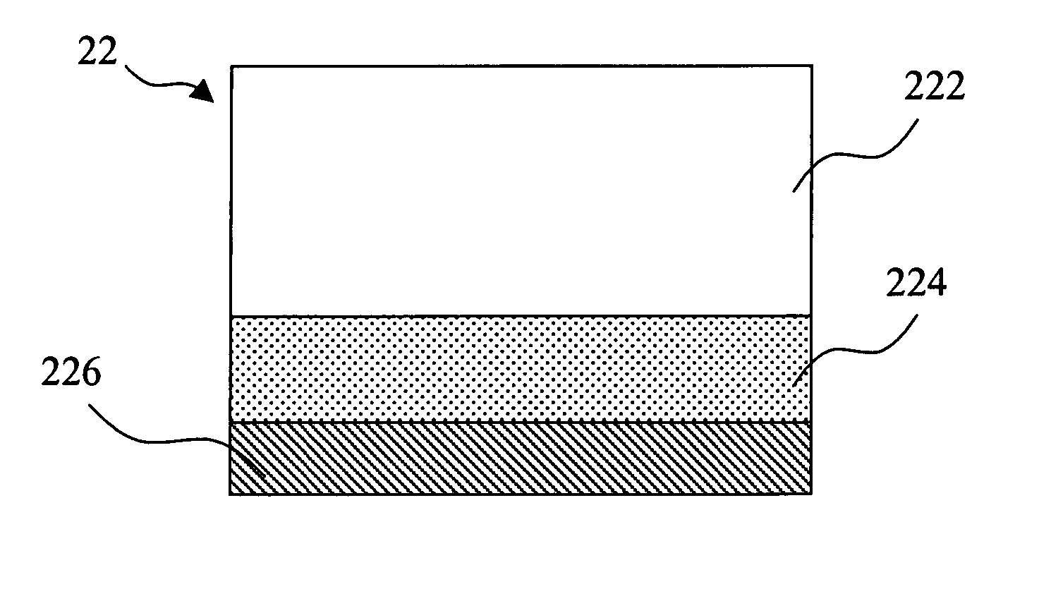
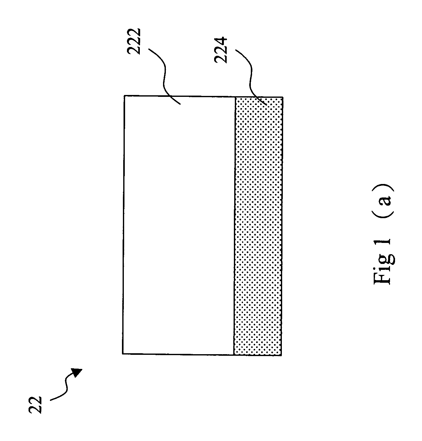
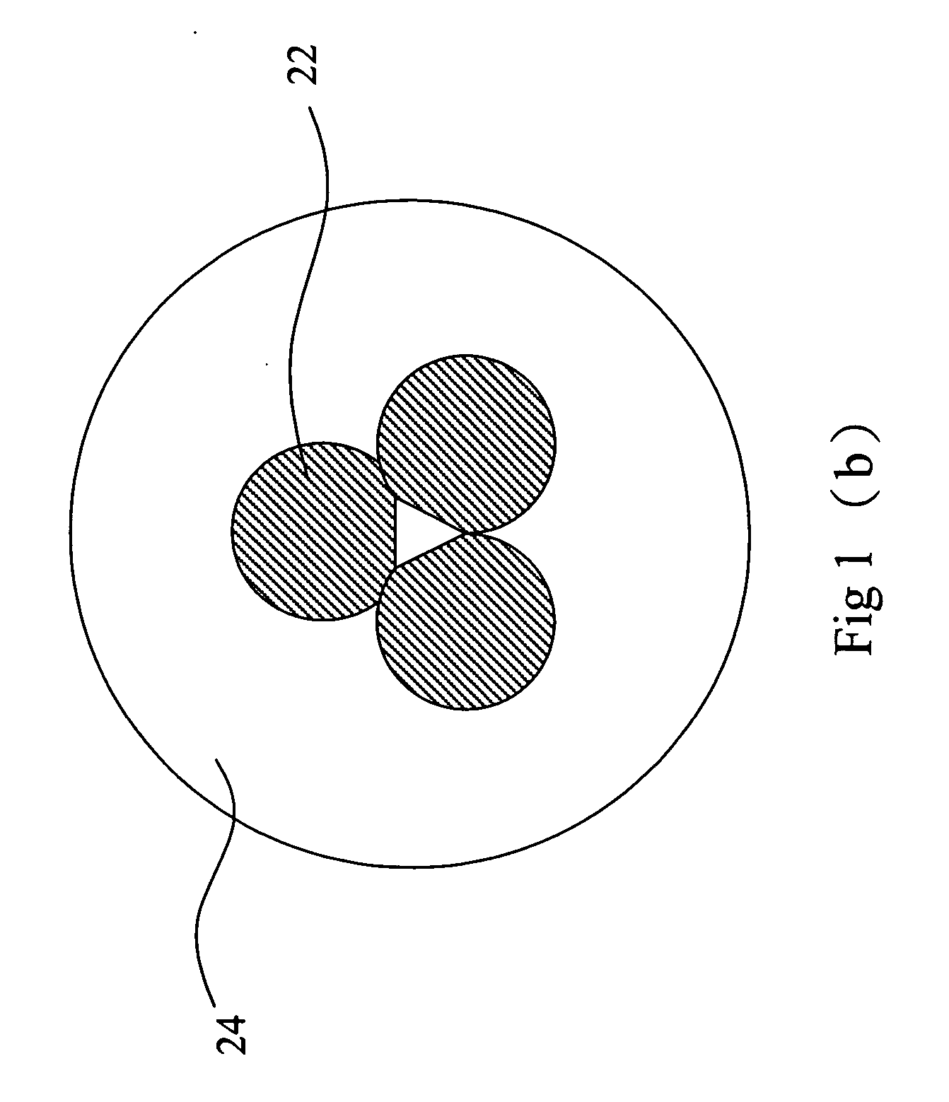
[0016] Refer to from FIG. 1(a) to FIG. 1(d) showing the steps of the grinding method for a sapphire wafer according to the present invention. In the present invention, three sapphire wafers 22 are firstly provided. As shown in FIG. 1(a), each sapphire wafer 22 comprises a substrate 222 and an electrically-conductive layer 224, wherein the substrate 222 is an insulation layer. Next, as shown in FIG. 1(b), those three sapphire wafers 22 are stuck to a fixing base 24 with a wax, and a pressure ranging from 1 to 10 kg / cm2 is applied to fix those sapphire wafers 22 onto the fixing base 24, wherein the fixing base 24 may be made of a ceramic material. Next, as shown in FIG. 1(c), the fixing base 24 is further fixed onto a machining table 26 via a vacuum-suction method, and the substrate 222 of the sapphire wafers 22 are roughly ground to a thickness of from 50 to 200 μm. Next, as shown in FIG. 1(d), a fine grinding follows, and the fixing base 24 is disposed on a polishing disc 28, and a ...


PUM


Abstract

The present invention discloses a grinding method for a sapphire wafer, wherein a sapphire wafer is firstly provided, and the sapphire wafer has a substrate and an electrically-conductive layer; the sapphire wafer is fixed onto a fixing base; the fixing base is further fixed to a machining table, and the substrate of the sapphire wafer is ground thereon; then, the fixing base is placed on a polishing disc, and the substrate is further thinned thereon; and lastly, the substrate is completely removed via an etching method. The present invention can shorten the time for removing the substrate of a sapphire wafer and also shorten the time for LED fabrication process; thus, the cost is reduced. Further, LED can work normally at high temperature, and the danger resulting from LED's working at high temperature can also be lessened.

Description

BACKGROUND OF THE INVENTION [0001] 1. Field of the Invention [0002] The present invention relates to a grinding method for a sapphire wafer, particularly to a grinding method for a sapphire wafer, which is applied to light emitting diodes. [0003] 2. Description of the Related Art [0004] LED (light emitting diode) is a luminescent light-emitting element and can convert electric energy into light energy in high efficiency. LED is also a tiny solid-state light source. LED primarily comprises a p-n junction of semiconductor, and when an appropriate voltage is applied to both ends of the p-n junction, the combination of electrons and electron holes will emit photons. LED has the advantages of miniature size, low power consumption, little heat generation, long service life, and superior vibration resistance. LED has been extensively used in daily living, such as illumination devices, backlight sources, advertisement signs, traffic signals, electric torches, camera flashlights, and decorat...

Claims


Application Information

Patent Timeline
Patent Type & Authority Applications(United States)
IPC IPC(8): H01L21/302
CPCC30B33/00C30B29/20
Inventor HSU, CHIH-MING
Owner CLEAVAGE ENTERPRISE
Why Eureka
Try Eureka