System and method for processing a substrate using supercritical carbon dioxide processing

a carbon dioxide and processing system technology, applied in the field of semiconductor manufacturing, can solve the problems of further difficulties in and the difficulty of processing films located in the trench

Inactive Publication Date: 2006-01-05
TOKYO ELECTRON LTD
View PDF98 Cites 62 Cited by
  • Summary
  • Abstract
  • Description
  • Claims
  • Application Information

AI Technical Summary

Problems solved by technology

Due to these aggressive trench dimensions, it can be difficult to process films located in the trench.
This presents further difficulties for processing films located in the trench.

Method used


Image

  • System and method for processing a substrate using supercritical carbon dioxide processing
  • System and method for processing a substrate using supercritical carbon dioxide processing
  • System and method for processing a substrate using supercritical carbon dioxide processing

Examples


Embodiment Construction

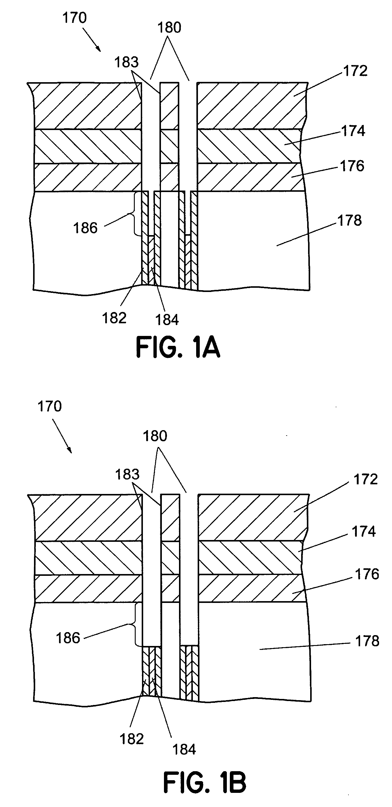
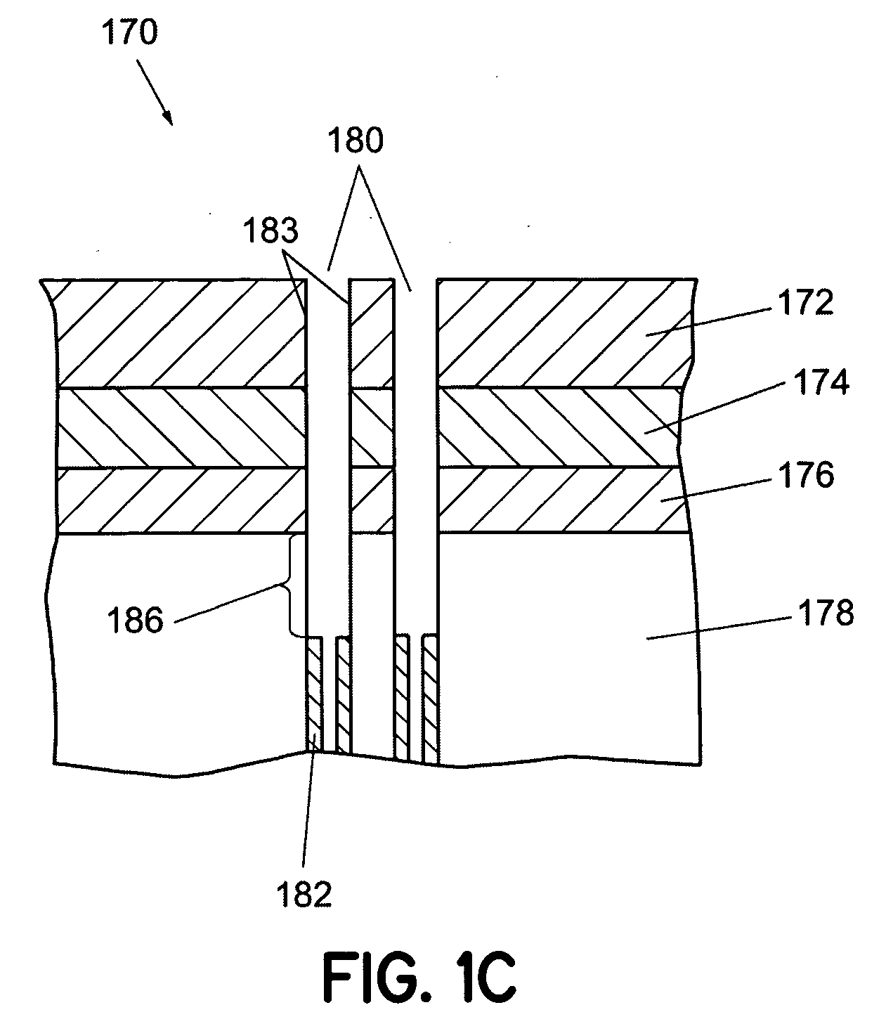
[0018] The term micro-feature, as used herein, refers to a feature formed in a substrate and / or in a layer or layers formed on a substrate that has dimensions on the micrometer scale, and typically the sub-micron scale, i.e., less than 1 μm. FIG. 1A schematically shows a cross-sectional view of a micro-feature containing a trench having a dielectric film on the sidewalls of the trench and a photoresist film covering a portion of the dielectric film according to an embodiment of the invention. The micro-feature 170 contains a hard mask film 172 (e.g., borosilicate glass, BSG), a pad nitride film 174, a pad oxide film 176, and a silicon substrate 178. The micro-feature 170 further contains a trench 180 that is formed by etching through the films 172 -176 and into the silicon substrate 178.

[0019] The trench 180 can be formed using a photolithographic process and dry etching techniques that are well known to persons skilled in the art of lithography and plasma etching. The exemplary tr...


PUM

PropertyMeasurementUnit
pressureaaaaaaaaaa
pressureaaaaaaaaaa
pressureaaaaaaaaaa

Abstract

A method and system for processing a substrate in a film removal system. The method includes providing the substrate in a substrate chamber of a film removal system, where the substrate has a micro-feature containing a dielectric film on a sidewall of the micro-feature and a photoresist film covering a portion the dielectric film, and performing a first film removal process using supercritical CO2 processing to remove the portion of the dielectric film not covered by the photoresist film. Following the first film removal process, a second film removal process using supercritical CO2 processing can be performed to remove the photoresist film. Alternately, wet processing can be used to perform one of the first film removal process or the second film removal process.

Description

FIELD OF THE INVENTION [0001] The invention relates to semiconductor manufacturing, and more particularly, to utilizing supercritical CO2 processing to remove a film from a micro-feature on a substrate. BACKGROUND OF THE INVENTION [0002] In the semiconductor industry, the minimum feature sizes of microelectronic devices are approaching the deep sub-micron regime to meet the demand for faster, lower power microprocessors and digital circuits. In the manufacturing of a trench capacitor for a dynamic random access memory (DRAM) device, a deep trench (DT) is etched several microns (μm) into a silicon substrate. During manufacturing of a deep trench capacitor, a dielectric film, such as doped silicon dioxide film (e.g., arsenic-doped silicon dioxide, also referred to as arsenosilicate glass (ASG)), is deposited on the sidewalls of the trench, in order to provide out-diffusion of the dopant (e.g., arsenic, As) from the doped dielectric film into the sidewalls of the silicon trench to form...

Claims


Application Information

Patent Timeline
Patent Type & Authority Applications(United States)
IPC IPC(8): H01L21/467C23F1/00H01L21/311
CPCH01L21/31133H01L21/31111
Inventor GALE, GLENNHILLMAN, JOSEPH T.JACOBSON, GUNILLAPALMER, BENTLEY
Owner TOKYO ELECTRON LTD
Why Eureka
Try Eureka