Thin film photovoltaic assembly method
- Summary
- Abstract
- Description
- Claims
- Application Information
AI Technical Summary
Benefits of technology
Problems solved by technology
Method used
Image

Examples
Embodiment Construction
[0023] The method of manufacturing of the present invention greatly improves the efficiency of manufacturing TFPPs. The present invention uses an adhesive layer that may be applied in a liquid to form the TFFP. A suitable adhesive layer in accordance with the present invention includes pumpable liquid adhesives, such as single, dual or multi-component hot-melts, thermosets, or reactive hot-melts.
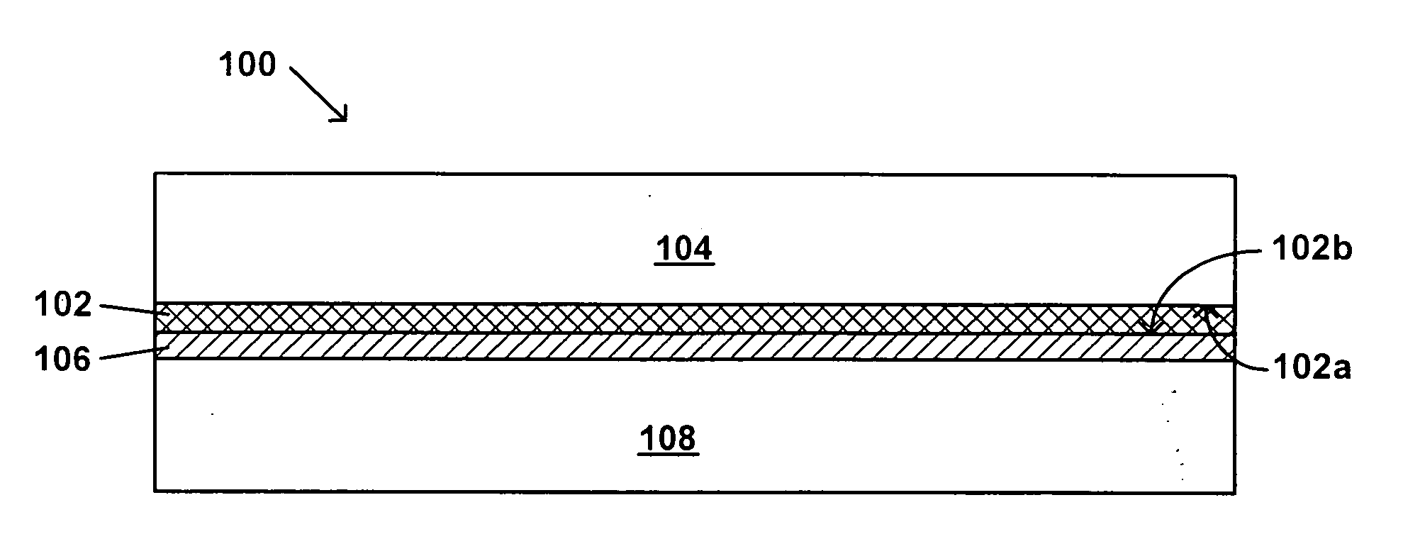
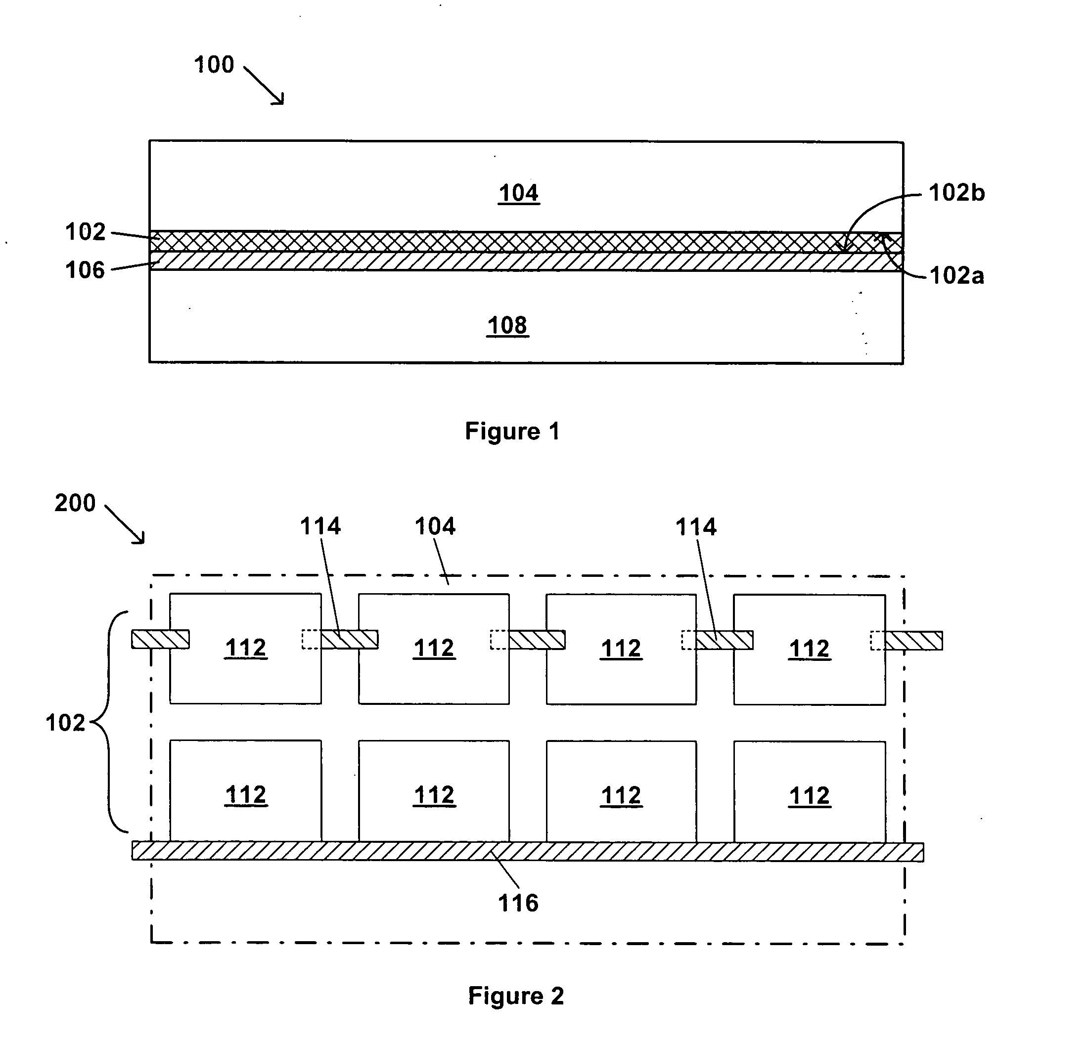
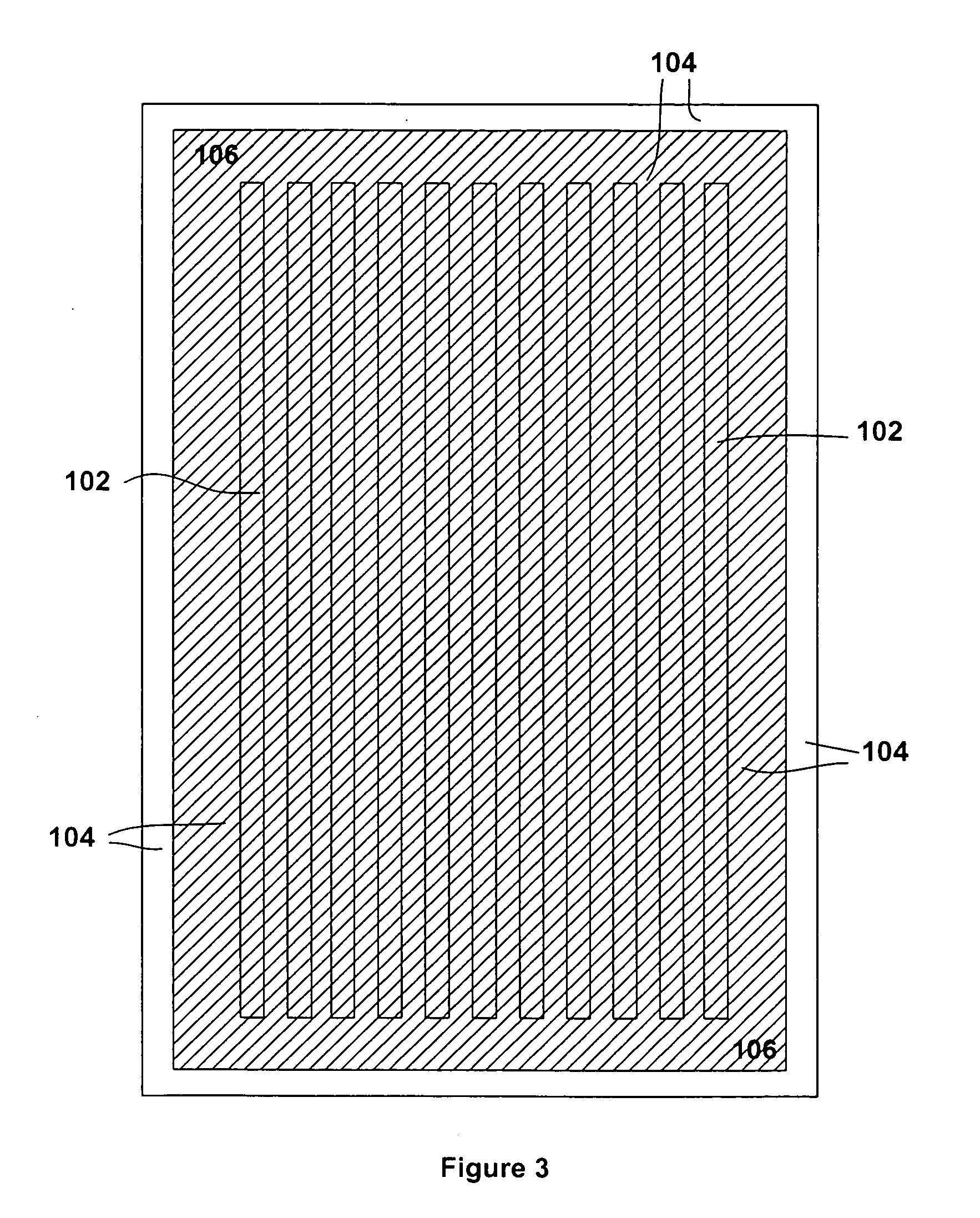
[0024] One embodiment of a thin film photovoltaic solar panel (TFPP) 100 in accordance with the present invention is shown in a cross-sectional schematic view in FIG. 1. The TFPP 100 includes a photovoltaic material layer 102. A first surface 102a of the photovoltaic material layer 102 is disposed on and attached to a transparent front panel (or substrate) 104. One of skill in the art will readily appreciate that the photovoltaic material layer 102 need not extend all the way to the edges of the front panel, but may only be disposed over a portion of the front panel. On a second surface 102...
PUM
 Abstract
Description
Claims
Application Information
 - Generate Ideas
- Intellectual Property
- Life Sciences
- Materials
- Tech Scout
- Unparalleled Data Quality
- Higher Quality Content
- 60% Fewer Hallucinations
Browse by: Latest US Patents, China's latest patents, Technical Efficacy Thesaurus, Application Domain, Technology Topic, Popular Technical Reports.
© 2025 PatSnap. All rights reserved.Legal|Privacy policy|Modern Slavery Act Transparency Statement|Sitemap|About US| Contact US: help@patsnap.com