

Display device
- Summary
- Abstract
- Description
- Claims
- Application Information
AI Technical Summary
Benefits of technology
Problems solved by technology
Method used
Image

Examples
embodiment
[0033] Embodiment Modes of the present invention will be described in detail with reference to the accompanying drawings. However, the invention is not limited to the following description and it is easily understood by those skilled in the art that various changes and modifications are possible, unless such changes and modifications depart from the content and the scope of the invention. Therefore, the invention is to be interpreted without limitation to the description in Embodiment Modes shown below. Note that, in the structure of the invention described hereinafter, the same reference numerals denote the same parts in different drawings.
[0034] The present invention relates to a structure of a display device having a plurality of pixels, in which when current higher than a current which can be controlled in a pixel (overcurrent) flows into a pixel, more current supplied into the pixel is selectively cut off or reduced. In order to achieve the object, a material by which the resi...
embodiment mode 1
[0039] In this embodiment mode, an example of a display device in which when overcurrent flows into a pixel, the current flowing into the pixel is cut off or reduced will be described below with reference to the drawing.
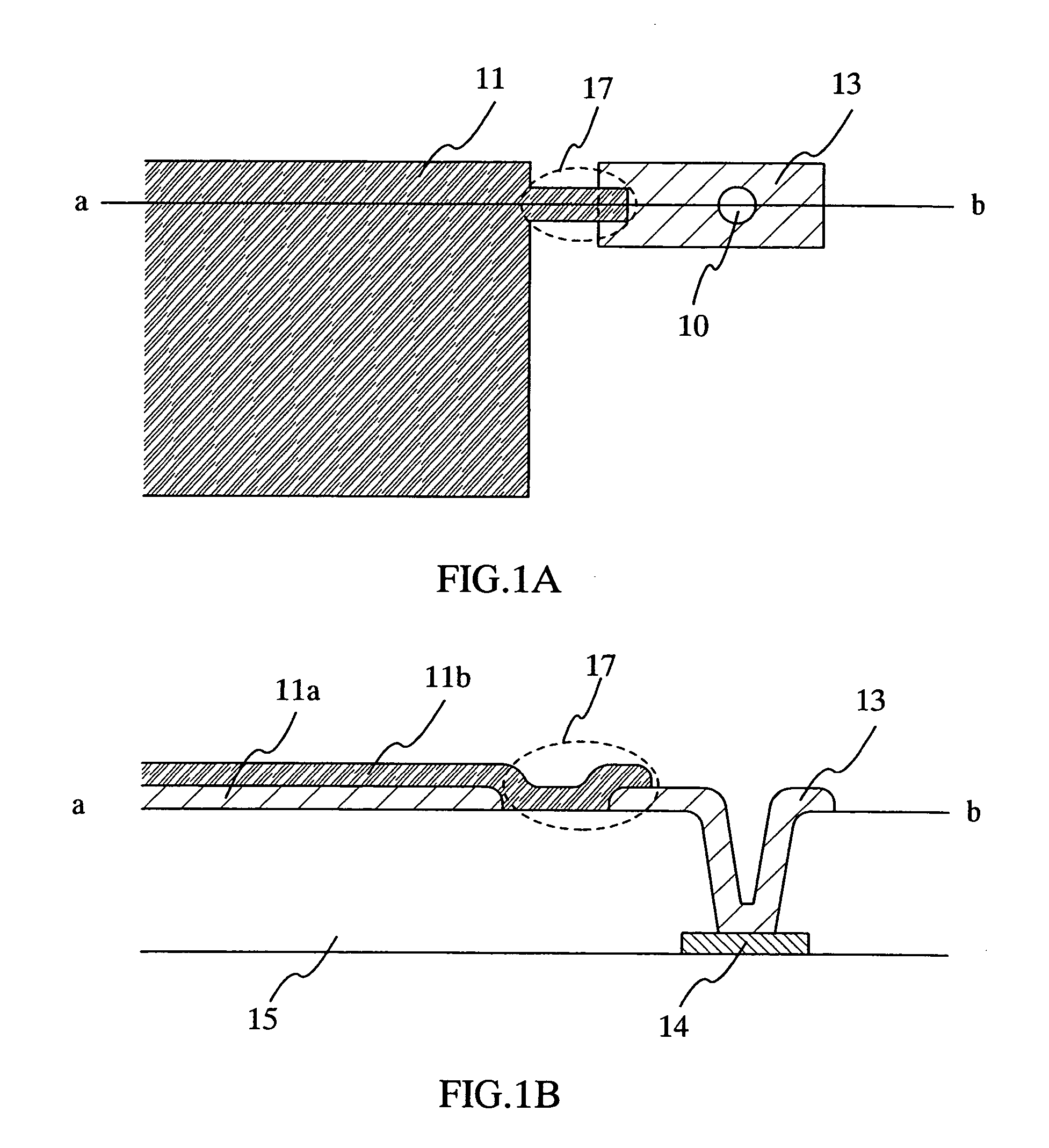
[0040] In FIGS. 1A and 1B, FIG. 1A shows a top view of a pixel electrode in a pixel of a display device, and FIG. 1B shows a cross-sectional view thereof. An interlayer insulating film 15 is formed so as to cover a wiring 14, and a contact hole 10 is formed in the interlayer insulating film 15. A pixel electrode 11 and the wiring 14 are electrically connected to each other through the contact hole 10. In this embodiment mode, the pixel electrode 11 except for a part thereof has a layered structure including a metal film 11a and a transparent electrode 11b. Here, the metal film 11a may have a single layer structure or a layered structure including an element selected from aluminum (Al), nickel (Ni), tungsten (W), molybdenum (Mo), titanium (Ti), platinum (Pt), copper ...
embodiment mode 2
[0058] In this embodiment mode, an example of a display device different from Embodiment Mode 1 will be described with reference to FIGS. 2A to 2C.
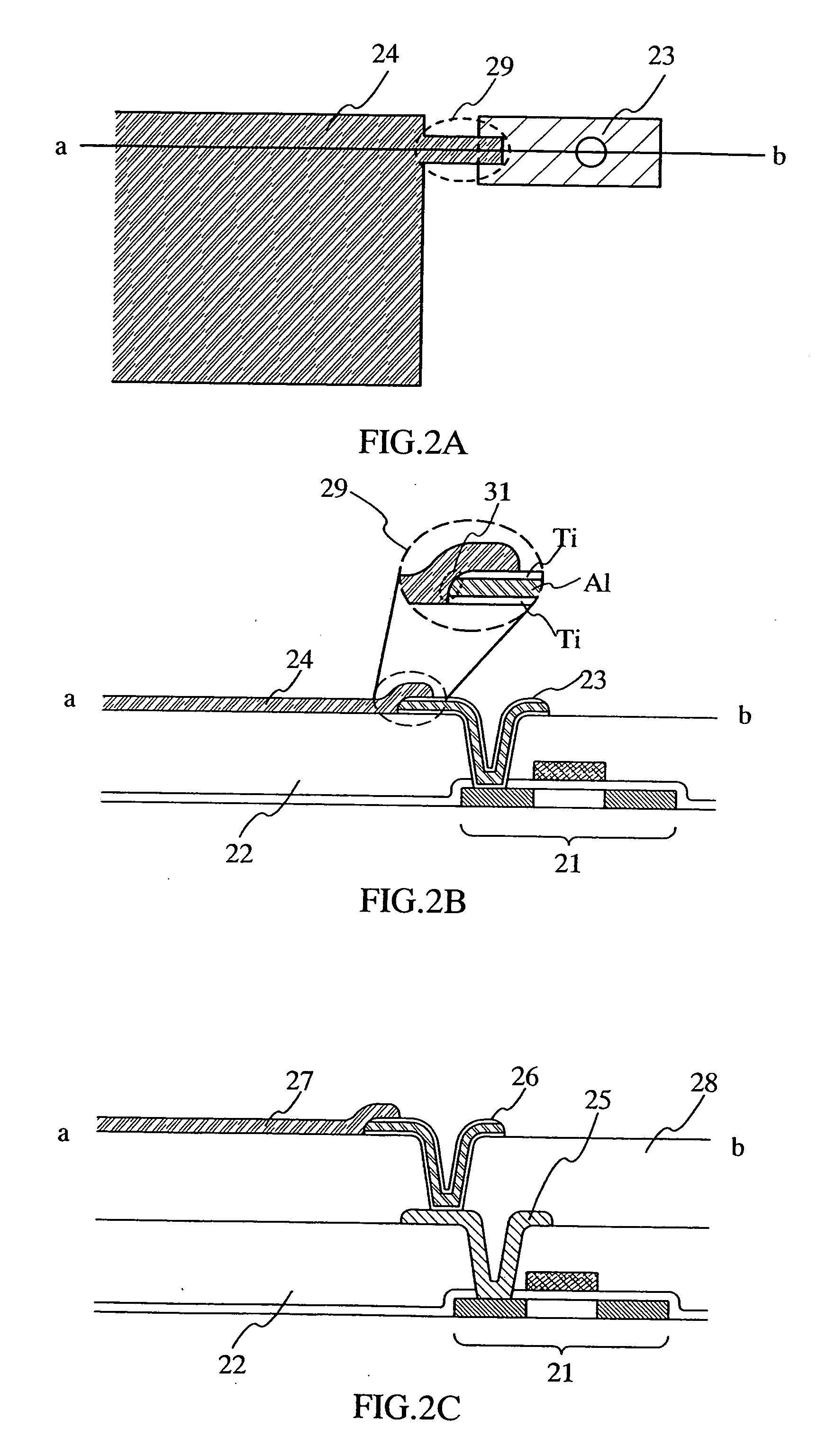
[0059] In FIGS. 2A to 2C, FIG. 2A shows a top view of a pixel electrode in a pixel of a display device, and FIG. 2B and FIG. 2C show a cross-sectional view thereof. A thin film transistor 21, an interlayer insulating film 22 covering the thin film transistor 21, and a wiring 23 over the interlayer insulating film 22 are formed. The wiring 23 is connected to the source or drain region of the thin film transistor 21 through a contact hole formed in the interlayer insulating film 22. Further, the pixel electrode 24 is electrically connected to the source or drain region of the thin film transistor 21 through the wiring 23. The wiring 23 may have a single layer structure or a layered structure including an element selected from aluminum (Al), nickel (Ni), tungsten (W), molybdenum (Mo), titanium (Ti), platinum (Pt), copper (Cu), tantalum (Ta)...
PUM
 Abstract
Description
Claims
Application Information