Method of manufacturing semiconductor device

a manufacturing method and semiconductor technology, applied in the direction of semiconductor devices, basic electric elements, electrical appliances, etc., can solve the problems of increasing lowering the resistance reducing the stability of the connection hole, so as to achieve the dual damascene processing. , the effect of easy carrying ou

Inactive Publication Date: 2006-01-12
SONY CORP
View PDF8 Cites 30 Cited by
  • Summary
  • Abstract
  • Description
  • Claims
  • Application Information

AI Technical Summary

Benefits of technology

[0032] In the method of manufacturing a semiconductor device according to the present invention, the organic sacrificing layer, the first mask layer and the second mask layer are sequentially laminated on the second insulation layer, i.e., the organic sacrificing layer is provided between the second insulation film and the first mask layer, so that the formation of wiring grooves in the second insulation film composed of an SiOC film, which has in related art been accompanied by difficulties in controlling the processed shapes, can be carried out easily, and the formation of a multi-layer wiring with low capacity and high performance can be realized without being influenced by the low dielectric constant film material applied to the second insulation film. Therefore, in the formation of a multi-layer wiring of the dual Damascene structure applied to the interlayer insulation film including the low dielectric constant film, it is possible to easily achieve the dual Damascene processing with little corner collapse and with the processing conversion difference controlled. This makes it possible to suppress or restrain the lowering in the yield of the product due to shortcircuits between the wirings, and to suppress or restrain the deterioration of the wiring reliability concerning initial defects due to insufficient withstand voltage, inter-wiring TDDB (Time Dependence Dielectric Breakdown), or the like. Besides, from the viewpoint of coping with miniaturization on the order of the 65 nm generation and the latter generations, also, the present invention making it possible to secure the space between wirings with good controllability promises the same effects as above. Furthermore, by combining the inventive method with a method of forming connection holes which are self-aligning relative to the wiring grooves, it is possible to manufacture a semiconductor device with a sufficient separation margin.
[0033] There is a need for a method of manufacturing a semiconductor device having a multi-layer wiring with high performance, high yield and high reliability by preventing defects due to shortcircuit with a different-potential wiring adjacent to connection holes, without sacrificing the opening properties and reliability of the connection holes, even in a minute multi-layer wiring in which a low dielectric constant film of the 65 nm generation or the latter generation is used. The need has been fulfilled by laminating an organic sacrificing layer, a first mask layer and a second mask layer on a second insulation film, since the margin in the thickness direction of the first mask layer can thereby be enlarged by the presence of the organic sacrificing layer, the accuracy in opening the wiring grooves and connection holes in the second insulation film can be enhanced, and the defects due to shortcircuit with the adjacent different-potential wiring can be thereby prevented.

Problems solved by technology

For example, the space between the wirings is reduced to a minimum of 100 nm under the 65 nm generation design rule and to about 70 nm under the 45 nm generation design rule, and it is difficult in principle to improve the misalignment in the lithography process by an amount corresponding to the reduction of the space.
In ordinary lithography processes, stable formation of the openings of the connection holes becomes considerably difficult when the opening size is reduced to 120 nm or less.
In addition, the degrees of difficulty in securing the wiring reliability concerning the subsequent filling-with-metal process, the lowering in resistance of the connection holes, stress migration, etc. are also raised.
Therefore, the final opening size tends to remain on the greater side as compared with the reduction ratio of the inter-wiring space, which leads to a further difficulty in securing the required space between the wirings.
Accordingly, the withstand voltage limit width tends to be rather enlarged, which again leads to a difficulty in securing the space between the wirings.

Method used


Image

  • Method of manufacturing semiconductor device
  • Method of manufacturing semiconductor device
  • Method of manufacturing semiconductor device

Examples


first embodiment

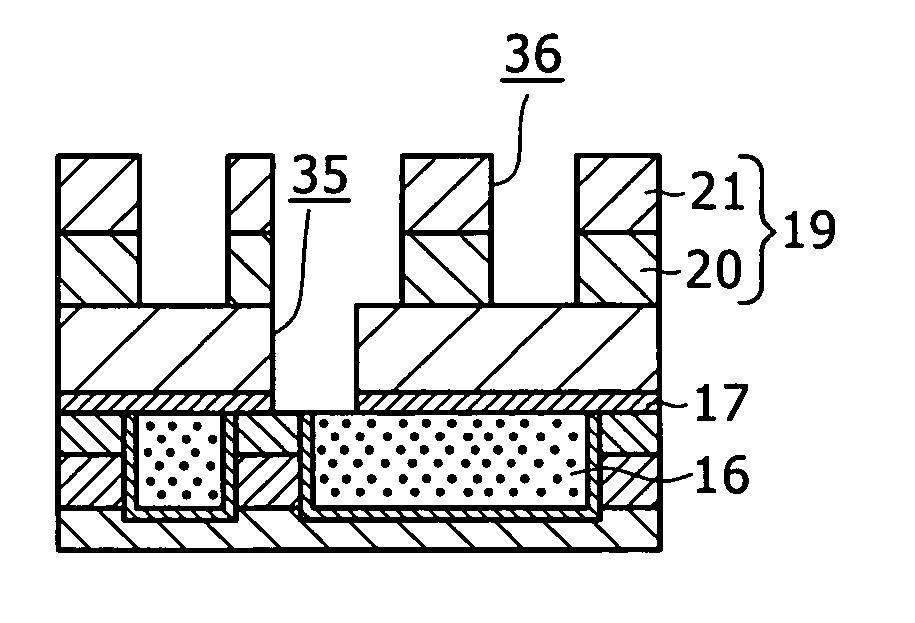
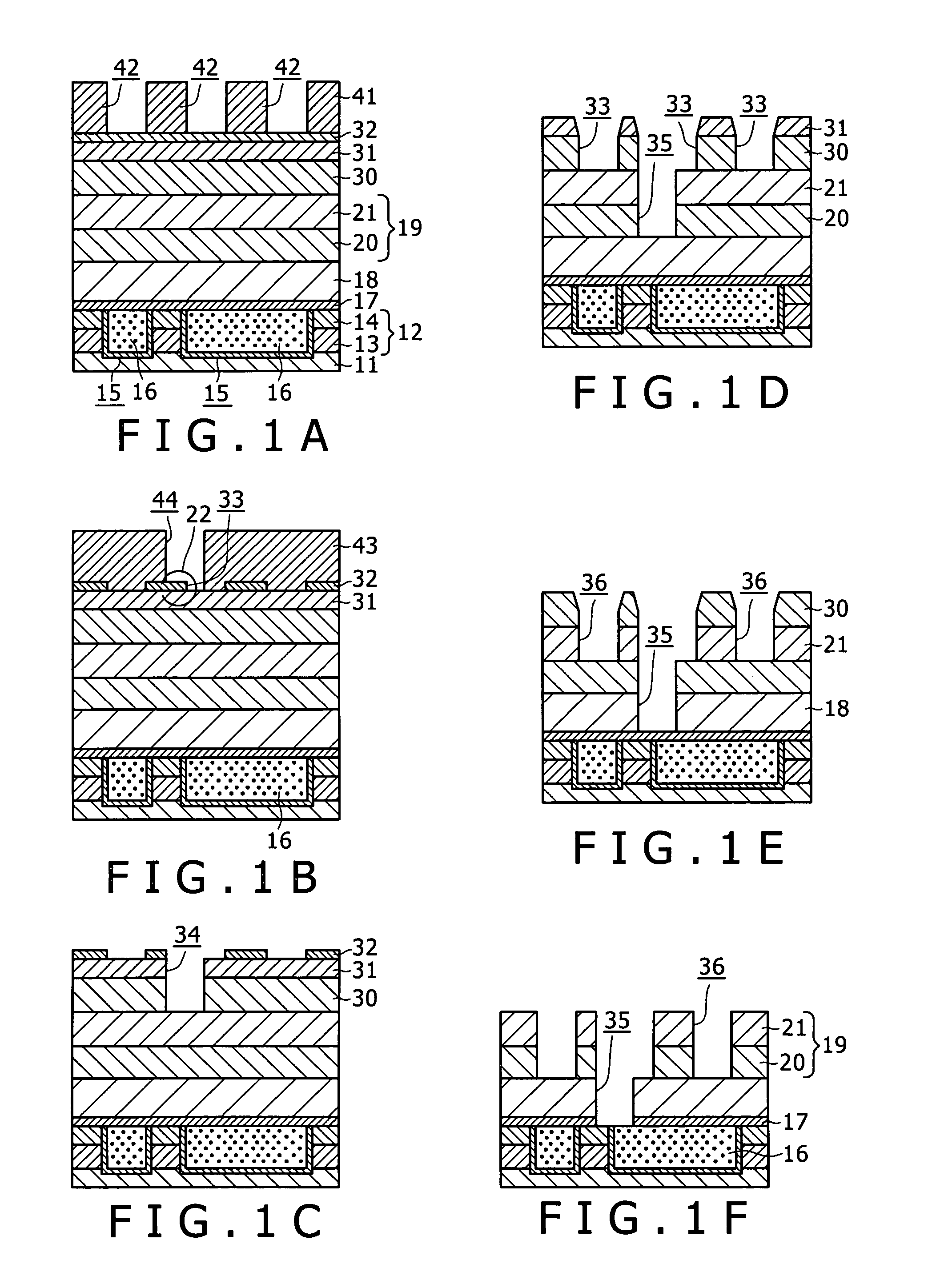
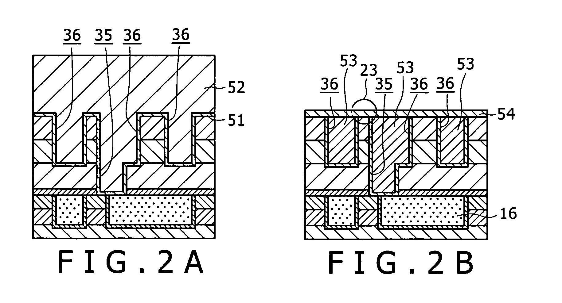
[0044] A first embodiment of the method of manufacturing a semiconductor device according to the present invention will be described referring to manufacturing step sectional views shown in FIGS. 1A to 1F and FIGS. 2A and 2B.

[0045] As shown in FIG. 1A, an interlayer insulation film 12 is formed on an under insulation film 11 deposited on a substrate (not shown). The interlayer insulation film 12 is formed, for example, by forming a laminate film including an organic film 13 and a silicon oxide (SiO2) film 14. The interlayer insulation film 12 is provided with a first wiring 16 in wiring grooves 15, with a close contact layer, a barrier metal layer or the like therebetween. The first wiring 16 is formed to have a wiring thickness of about 150 nm by burying a copper (Cu) film, for example. In addition, an oxidation inhibitive layer 17 is formed on the first wiring 16. The oxidation inhibitive layer 17 is formed, for example, by forming a silicon carbide (SiC) film in a thickness of 3...

second embodiment

[0072] A second embodiment of the method of manufacturing a semiconductor device according to the present invention will be described referring to manufacturing step sectional views shown in FIGS. 3A to 3F and FIGS. 4A and 4B. While in the embodiment 1 the prevention of shortcircuit defects between the wiring and the connection holes and the securing of the withstand voltage were realized by improving the corner collapse shape of the wiring grooves through the laminate etching mask structure including the organic sacrificing layer, in the cases of the 32 nm generation and the latter generations there is a need for miniaturization on the order of half-pitch≦60 nm and a dielectric constant reduction on the order of dielectric constant≦2.2. In view of this, in the second embodiment, based on the manufacturing method in the embodiment 1, one example of a method of manufacturing a multi-layer wiring through a groove wiring structure applicable to the formation of a wiring with a minute p...

third embodiment

[0101] A third embodiment of the method of manufacturing a semiconductor device according to the present invention will be described referring to manufacturing step sectional views shown in FIGS. 5A to 5F and FIGS. 6A and 6B. While the manufacturing method in the so-called hybrid low dielectric constant film structure in which an organic film (for example, a polyaryl ether film) is sandwiched between the wiring layers has been described in the embodiments 1 and 2 above, the present invention is applicable also to the cases of other low dielectric constant film structures. Here, an example of application to a low dielectric constant film structure based primarily on an SiOC film will be described.

[0102] As shown in FIG. 5A, an interlayer insulation film 12 is formed on an under insulation film 11 deposited on a substrate (not shown). The interlayer insulation film 12 is formed, for example, by forming a laminate film composed of an organic film 13 and a silicon oxide (SiO2) film 14....


PUM


Abstract

A method of manufacturing a semiconductor device, including the steps of: forming first and second insulation films on a substrate; sequentially forming an organic sacrificing layer and first and second mask layers thereon; forming a wiring groove pattern in the second mask layer; forming a connection hole pattern for forming connection holes in the second and first mask layers and the organic sacrificing layer; forming a wiring groove pattern in the first mask layer and the organic sacrificing layer and forming the connection holes in the second insulation film, by etching conducted by use of the second and first mask layers as an etching mask; and forming the wiring grooves in the second insulation film and forming the connection holes in the second and first insulation films, by use of the first mask layer and the organic sacrificing layer as a mask.

Description

BACKGROUND OF THE INVENTION [0001] The present invention relates to a method of manufacturing a semiconductor device by which miniaturization of a wiring and enhancement of the degree of integration are facilitated while securing a voltage resistance between conductor layers used for wiring. [0002] Attendant on the miniaturization of and enhancement of the degree of integration of semiconductor devices, the delay of electric signals due to the time constant of the wiring becomes a serious problem. For the conductor layers used in a multi-layer wiring step, the copper (Cu) wiring has come to be introduced in place of the wiring formed by use of an aluminum (Al) based alloy. Unlike the metallic materials used in the past for multi-layer wiring structures such as aluminum, copper is difficult to pattern by etching and, therefore, the so-called groove wiring technology (e.g., the Damascene process) is generally used in which wiring grooves are preliminarily formed between layers and are...

Claims


Application Information

Patent Timeline
Patent Type & Authority Applications(United States)
IPC IPC(8): H01L21/4763
CPCH01L21/76811H01L21/76835H01L21/76816H01L21/76813H01L21/768
Inventor KANAMURA, RYUICHI
Owner SONY CORP
Why Eureka
Try Eureka