Organic electroluminescent element and display device using the same

a technology of electroluminescent elements and display devices, applied in the direction of discharge tube luminescnet screens, other domestic articles, natural mineral layered products, etc., can solve the problems of significant durability degradation, and achieve the effect of improving durability and consuming a large amount of energy

Active Publication Date: 2006-01-19
UDC IRELAND
View PDF7 Cites 10 Cited by
  • Summary
  • Abstract
  • Description
  • Claims
  • Application Information

AI Technical Summary

Benefits of technology

[0015] This is because, in other words, when the ionization potential of the material contained in the hole blocking layer is high, a larger amount of energy is required for injecting holes, and when a large amount of energy is required for injecting holes, it is expected that the hole blocking layer would be unstable with respect to the holes. It can be anticipated therefrom that durability can be improved by using a material of low ionization potential in the hole blocking layer.

Problems solved by technology

If the amount of holes near the hole blocking layer is increased, it is expected that using a material with high ionization potential as the hole blocking layer would lead to significant deterioration of durability.

Method used


Image

  • Organic electroluminescent element and display device using the same
  • Organic electroluminescent element and display device using the same
  • Organic electroluminescent element and display device using the same

Examples


example 1

[0102] On a glass substrate having a transparent conductive film of indium.tin oxide (ITO) deposited thereon to a thickness of 150 nm (manufactured by Geomatech), an anode was formed by performing patterning via photolithography and hydrochloric acid etching. The pattern-formed ITO substrate was subjected to ultrasonic cleaning in acetone, washing with pure water and ultrasonic cleaning in isopropyl alcohol in the described order, then to drying by nitrogen blowing and finally to ultraviolet ozone cleaning. The thus treated substrate was placed in a vacuum deposition apparatus. Subsequently, a vacuum was drawn until the degree of vacuum in the deposition apparatus was lowered to 2.7×10⁻⁴ Pa or less.

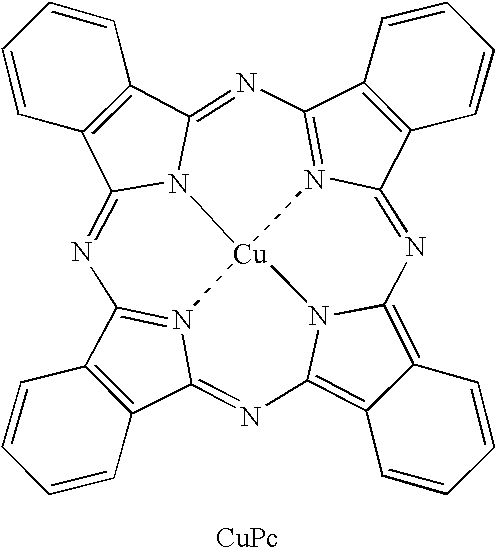
[0103] Subsequently, copper phthalocyanine (CuPc) represented below was heated in the deposition apparatus, and deposition was carried out at a deposition rate of 0.1 nm / sec, to form a hole injecting layer having a thickness of 10 nm.

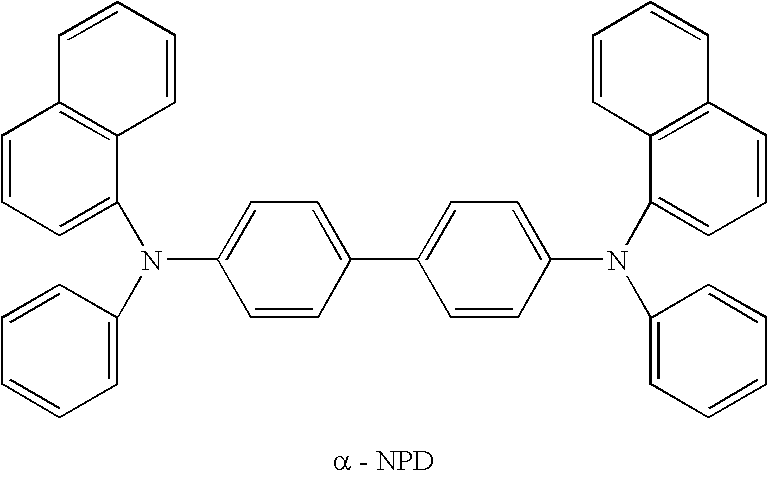
[0104] Next, on the thus formed hole injecting layer...

example 2

[0119] An organic EL element was prepared in the same manner as in Example 1, except that the thickness of the hole transport layer as formed in Example 1 was changed to 25 nm, and the same measurements were carried out as in Example 1.

[0120] The maximum wavelength of the luminescence spectrum of the element that was obtained according to Example 2 was 583 nm, which was identified to be derived from the dopant B.

example 3

[0121] An organic EL element was prepared in the same manner as in Example 1, except that the thickness of the hole transport layer as formed in Example 1 was changed to 10 nm, and the same measurements were carried out as in Example 1. The maximum wavelength of the luminescence spectrum of the element that was obtained according to Example 3 was 584 nm, which was identified to be derived from the dopant B.


PUM

PropertyMeasurementUnit
thicknessaaaaaaaaaa
ionization potentialaaaaaaaaaa
thicknessaaaaaaaaaa

Abstract

The present invention provides an organic electroluminescent element including an anode, a cathode, and a plurality of organic compound layers including at least one organic luminescent layer between the anode and the cathode, in which the organic luminescent layer contains a host material and two or more phosphorescent materials; the organic luminescent layer is adjacent to the organic compound layers at both an anode side and a cathode side thereof; the organic compound layer disposed adjacent to the organic luminescent layer at the anode side thereby has a thickness of 50 nm or less in thickness; and the organic compound layer disposed adjacent to organic luminescent layer at the cathode side thereby contains a compound having an ionization potential of 6.0 eV or less. The present invention also provides a display device using the organic electroluminescent element.

Description

CROSS-REFERENCE TO RELATED APPLICATION [0001] This application claims priority under 35 USC 119 from Japanese Patent Applications No. 2004-208983 and 2005-84945, the disclosure of which is incorporated by reference herein. BACKGROUND OF THE INVENTION [0002] 1. Field of the Invention [0003] The present invention relates to an organic electroluminescent element and a display device using the same. [0004] 2. Description of the Related Art [0005] Organic luminescent elements employing organic materials are expected to be promising in applications such as inexpensive, full-color, wide flat-panel display devices of the solid luminescent type and writing light source arrays, and thus development of the elements has been carried out extensively. An organic luminescent element in general consists of a luminescent layer, and a pair of opposing electrodes between which the luminescent layer is disposed. When an electric field is applied between the two electrodes, electrons are injected from t...

Claims


Application Information

Patent Timeline
Patent Type & Authority Applications(United States)
IPC IPC(8): H05B33/12
CPCH01L51/006H01L51/0071H01L51/0078H01L51/0081H01L2251/558H01L51/009H01L51/0094H01L51/5016H01L51/5048H01L51/0087Y10S428/917H10K85/633H10K85/311H10K85/361H10K85/346H10K85/324H10K85/657H10K85/40H10K50/14H10K50/11H10K2101/10H10K2102/351
Inventor KITAMURA, YOSHITAKAYAMAZAKI, KAZUKIMISHIMA, MASAYUKI
Owner UDC IRELAND
Why Eureka
Try Eureka