Electronic part-containing elements, electronic devices and production methods

a technology of electronic devices and components, applied in the field of electronic parts containing or built-in elements, can solve the problems of inability to adapt, increase the thickness of the layer in which parts with large thicknesses are buried, and the production process can only be carried out under low-temperature conditions, so as to reduce the thickness of the package and reduce the thickness of the device. , the effect of size and weigh

Inactive Publication Date: 2006-01-26
SHINKO ELECTRIC IND CO LTD
View PDF1 Cites 17 Cited by
  • Summary
  • Abstract
  • Description
  • Claims
  • Application Information

AI Technical Summary

Benefits of technology

[0012] The present invention is directed to solve the above-mentioned prior art problems, and has an object to provide an electronic device which highly densely mounts active elements such as semiconductor elements and passive elements such as resistors and capacitors making it possible to decrease the thickness, size and weight of the device, contributing to decreasing the thickness of the package, permitting a low-temperature production process to be applied, and making it possible to form an LCR circuit in one build-up layer without using the whole surface of the substrate for forming the passive elements, as well as a novel electronic part-containing element useful for the manufacture of the electronic devices.

Problems solved by technology

In the above part-containing module, however, ready-made active parts and passive parts are buried therein causing a problem of an increased thickness of the layer in which parts having large thicknesses are buried.
However, the following problems exist when the passive elements are fabricated between the layers and in the core during the process of producing the semiconductor device according to the above-mentioned method.
1) The production process can be carried out only under low-temperature conditions and cannot be adapted to a high-temperature production process of not lower than 200° C. that has been demanded in recent years.
2) The passive elements must be formed by using the whole surface of the motherboard to increase the cost of production due to the use of an expensive material for forming the passive elements.
3) Each passive element is formed through a different process and, hence, it is difficult to form a circuit (an LCR circuit) mounting, for example, an inductor, a capacitor and a resistor in one build-up layer.

Method used


Image

  • Electronic part-containing elements, electronic devices and production methods
  • Electronic part-containing elements, electronic devices and production methods
  • Electronic part-containing elements, electronic devices and production methods

Examples


examples

[0090] Next, examples of the present invention will now be described with reference to the accompanying drawings. It should be noted that the present invention is not limited to these examples only.

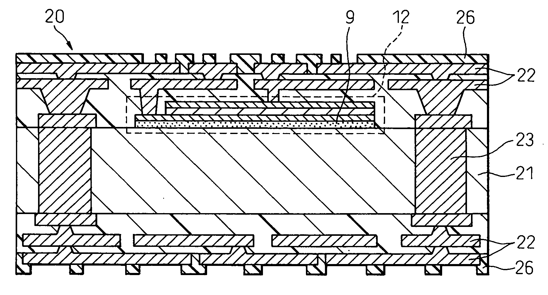
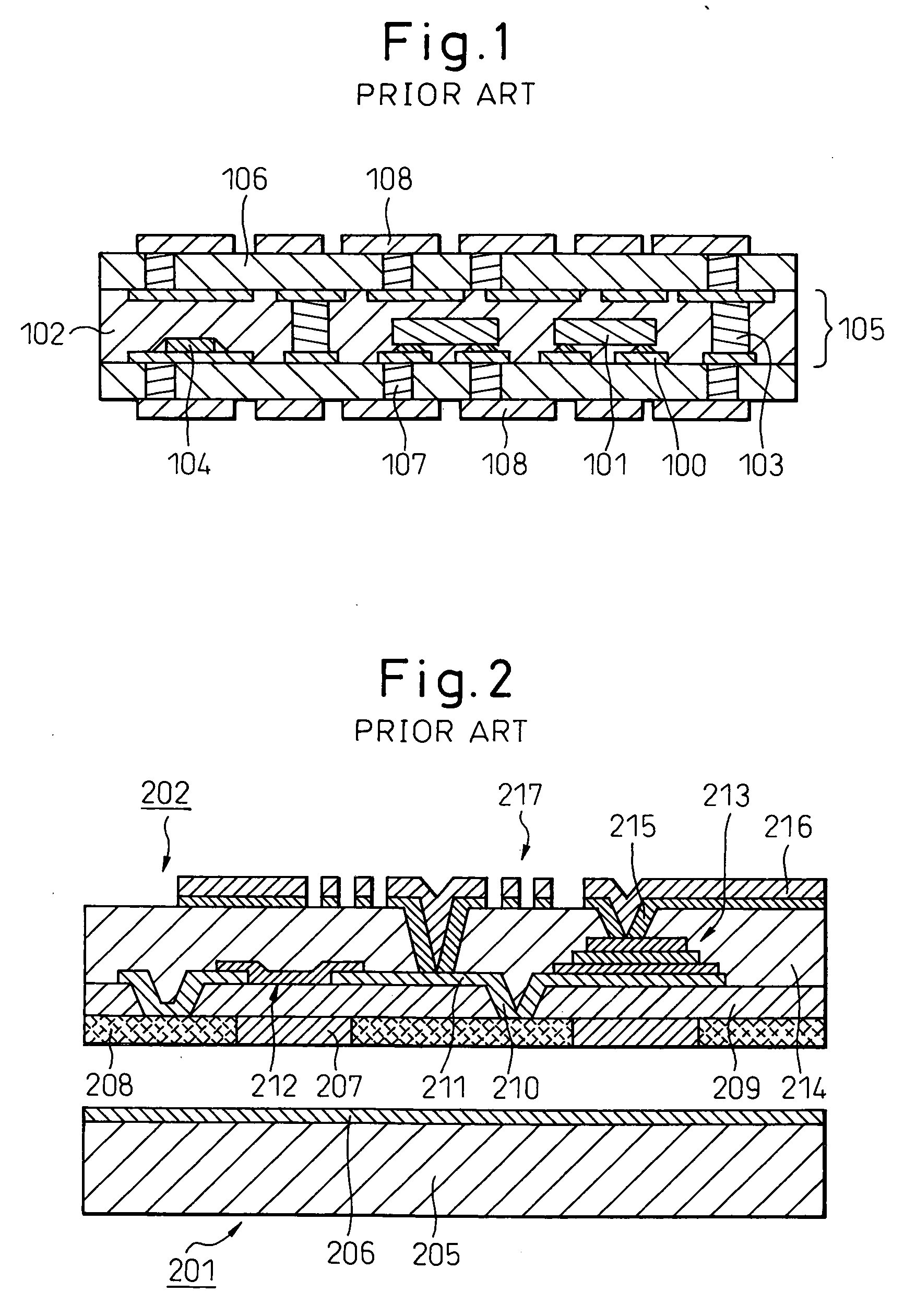
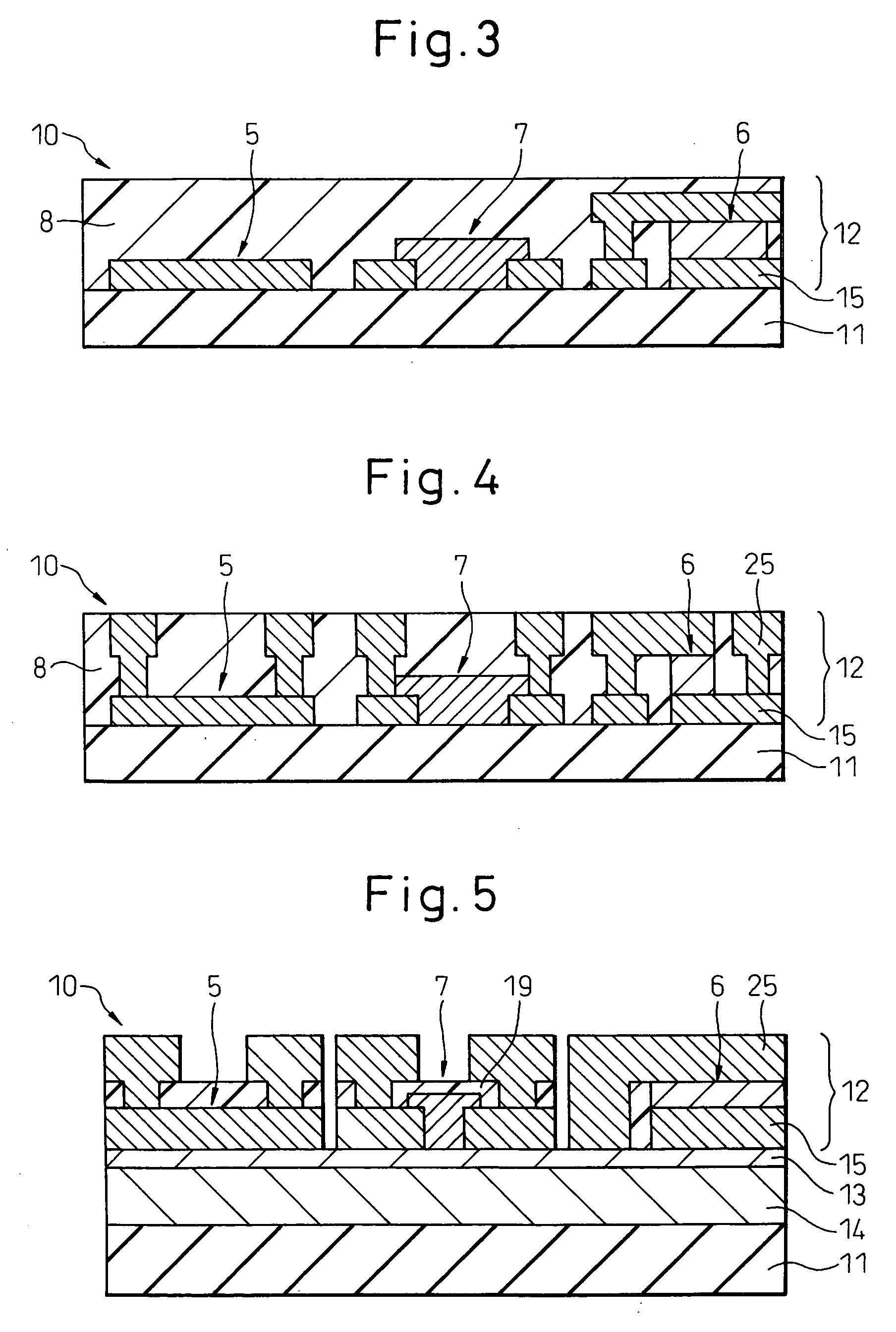
[0091]FIG. 3 is a sectional view illustrating a preferred embodiment of the electronic part-containing element of the present invention. The electronic part-containing element 10 comprises a support member 11 and a sheet-like circuit module 12 supported thereby. The support member 11 is removed in the step of producing an electronic device. A glass board is used in this embodiment. The circuit module 12 includes a composite circuit (LCR circuit) of a spiral inductor 5, a capacitor 6 and a resistor 7. The LCR circuit is in the form of a thin film as shown and contributes to decreasing the size of the device. Of the surfaces of the circuit module 12, the surface that comes in contact with the support member 11 is provided with a connection terminal (lower electrode) 15.

[0092] In the illus...


PUM


Abstract

An electronic part-containing element used by being incorporated in an electronic device, in which the electronic part-containing element comprises an insulating support member which does not take part in the constitution of the electronic device but is removed in the process of producing the electronic device, and a circuit module supported by the support member, and the circuit module contains one or more electronic parts, each in the form of a thin film, therein and has connection terminals for the electronic part at least on the surface thereof that comes into contact with the support member.

Description

BACKGROUND OF THE INVENTION [0001] 1. Field of the Invention [0002] The present invention relates to an electronic part-containing or built-in element used, while being buried in, for example, a wiring board, in the production of electronic devices such as semiconductor devices, to a method of producing the same, to an electronic device incorporating the electronic part-containing element of the present invention, and to a method of producing the same. [0003] 2. Description of the Related Art [0004] In recent years, to satisfy the requirements of high performance, high degree of function, small size and decreased weight of electronic equipments and other devices, efforts have been made to improve both the constitution of the devices and the production processes concerning semiconductor devices and other electronic devices. In semiconductor devices, for example, it is a widely accepted practice to very densely mount active elements such as semiconductor elements and passive elements ...

Claims


Application Information

Patent Timeline
Patent Type & Authority Applications(United States)
IPC IPC(8): H01L29/00
CPCH01L21/6835H01L2924/014H01L24/18H01L24/82H01L2224/18H01L2924/01002H01L2924/01013H01L2924/01027H01L2924/01029H01L2924/01073H01L2924/01074H01L2924/01078H01L2924/04953H01L2924/09701H01L2924/19041H01L2924/19042H01L2924/19043H05K1/141H05K1/16H05K1/185H05K3/20H05K3/4602H05K2201/0317H05K2201/10045H05K2203/016H01L2924/01005H01L2924/01006H01L2924/01024H01L2924/01033H01L2924/01055H01L23/5389
Inventor OI, KIYOSHIHORIKAWA, YASUYOSHITAKANO, AKIHITO
Owner SHINKO ELECTRIC IND CO LTD
Why Eureka
Try Eureka