Robust fluorine containing Silica Glass (FSG) Film with less free fluorine

a technology silica glass, which is applied in the direction of semiconductor devices, semiconductor/solid-state device details, electrical equipment, etc., can solve the problems of loss of adhesion between the low-k film and the ta liners, instability of fsg dielectric film, and concern for propagation delay, etc., to achieve less free, less porous, and improved film quality

Inactive Publication Date: 2006-01-26
TAIWAN SEMICON MFG CO LTD
View PDF9 Cites 3 Cited by
  • Summary
  • Abstract
  • Description
  • Claims
  • Application Information

AI Technical Summary

Benefits of technology

[0013] Advantages of embodiments of the invention include providing a fluorine containing dielectric film for use as a dielectric material layer in semiconductor devices that has less free F and is compatible with the conductive materials used in modern interconnect systems. The fluorine containing dielectric film is less porous, is more stable and has an improved film quality than prior art FSG dielectric films. Semiconductor devices using the novel fluorine containing dielectric film have improved electrical performance, such as reduced contact resistance of vias (Rc-Via).

Problems solved by technology

As semiconductor devices are scaled down in size, the propagation delay, or the RC delay, becomes a concern.
The evolution of F from the FSG oxide is a problem when used in copper interconnect systems, for example, because the F readily attacks Ta-based liners of the copper interconnects, leading to volatile TaF2 formation and resulting in the loss of adhesion between the low-k film and the Ta liners.
FSG dielectric films with a high F concentration have been shown to be unstable, resulting in blistering after depositing a cap layer and / or metal layer, and also after passivation and metallization alloying treatments.
Another problem with prior art FSG dielectric films is that they are porous, being greater than about 5% porous (defined as 5%+ for following description), which causes the FSG dielectric films to be unstable.
The use of prior art FSG dielectric films in semiconductor devices can result in metal shorts or metal bridging, high leakage current between metal, and stress migration failures.

Method used


Image

  • Robust fluorine containing Silica Glass (FSG) Film with less free fluorine
  • Robust fluorine containing Silica Glass (FSG) Film with less free fluorine
  • Robust fluorine containing Silica Glass (FSG) Film with less free fluorine

Examples


Embodiment Construction

[0023] The making and using of the presently preferred embodiments are discussed in detail below. It should be appreciated, however, that the present invention provides many applicable inventive concepts that can be embodied in a wide variety of specific contexts. The specific embodiments discussed are merely illustrative of specific ways to make and use the invention, and do not limit the scope of the invention.

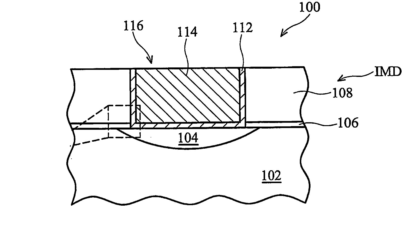
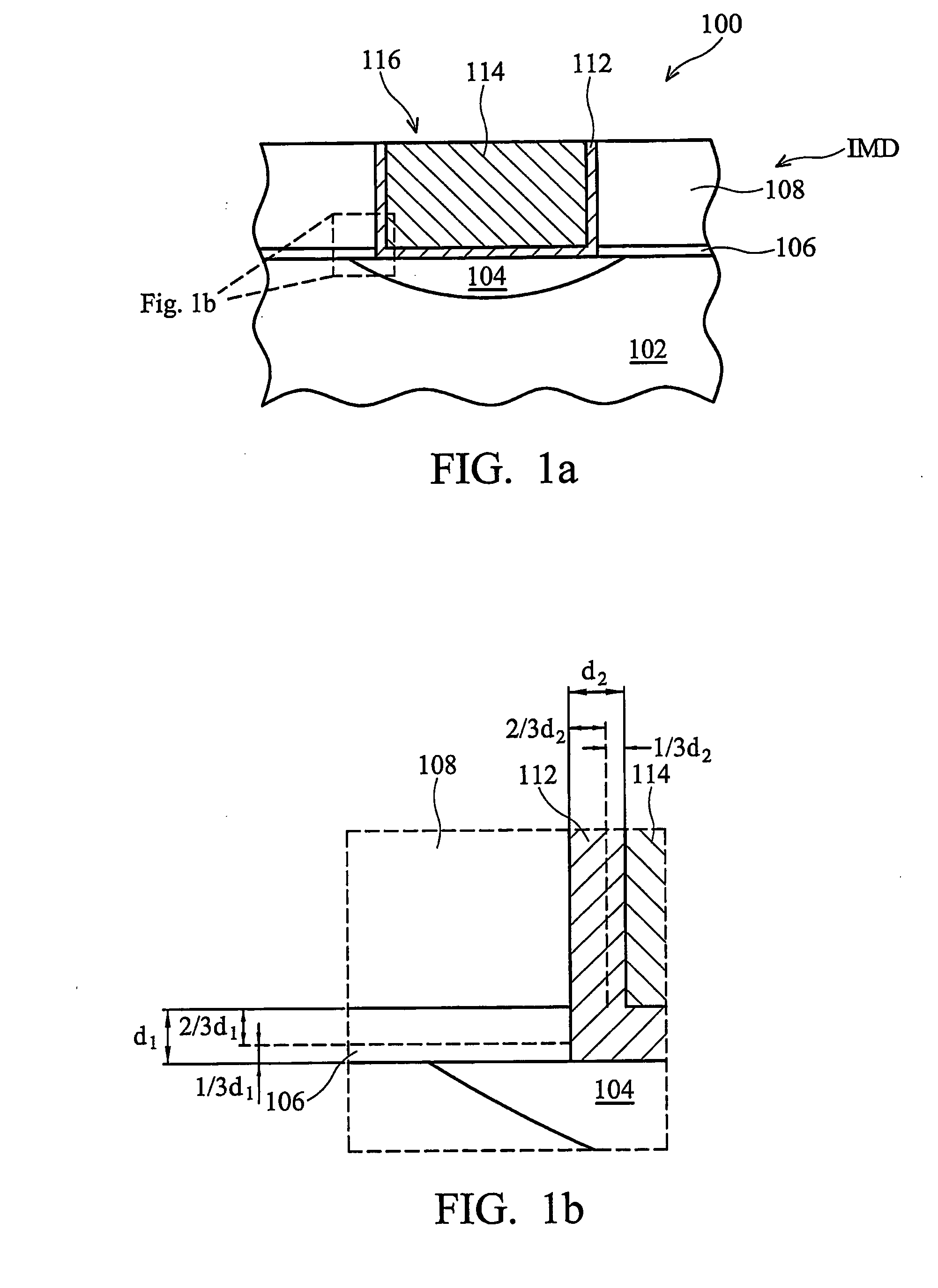
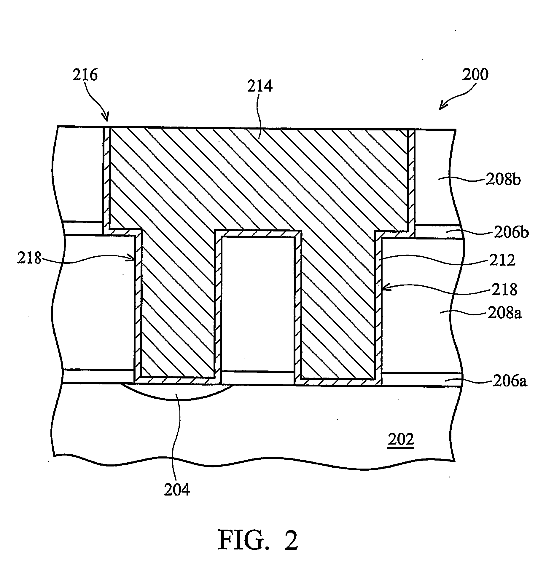
[0024] The present invention will be described with respect to preferred embodiments in a specific context, namely a fluorine containing or FSG dielectric film having less free F formed on a semiconductor substrate or workpiece. Embodiments of the invention may also be applied, however, to other applications and technologies where dielectric materials are used.

[0025] Free fluorine, or fluorine that has not bonded chemically with silicon, is found in a high percentage in prior art FSG dielectric films. For example, prior art FSG dielectric films may comprise greater than ab...


PUM

PropertyMeasurementUnit
dielectric constantaaaaaaaaaa
temperatureaaaaaaaaaa
partial pressureaaaaaaaaaa

Abstract

A semiconductor device and method of manufacture thereof having a less free fluorine (F) fluorine containing Silica Glass (FSG) dielectric film formed thereon. The FSG dielectric film includes about 25% or less free F, has a porosity of about 5% or less and has a dielectric constant of about 3.8 or less. A first barrier layer may be disposed between a workpiece and the FSG dielectric film, and a second barrier layer may be disposed between the FSG dielectric film and at least one conductive line formed in the FSG dielectric film. The FSG dielectric film is formed by introducing SiF4:SiH4 at a reaction condition ratio of about 2.5 or less at a pressure of about 3 Torr or less and at an RF of about 500 watts to 5000 watts.

Description

[0001] This application claims the benefit of U.S. Provisional Application No. 60 / 589,240, filed on Jul. 20, 2004, entitled “Robust Fluorinated Silica Glass (FSG) Film with Less Free Fluorine,” which application is hereby incorporated herein by reference.TECHNICAL FIELD [0002] The present invention relates generally to the fabrication of semiconductor devices, and more particularly to the formation of fluorine containing dielectric films. BACKGROUND [0003] Semiconductor devices are fabricated by depositing and patterning one or more conductive, insulating, and semiconductor layers to form integrated circuits. Some integrated circuits have multiple layers (or multilevels) of interconnect. The dielectric layers between metal levels are referred to in the art as inter-metal dielectrics (IMD's). Using multilevel interconnects results in the ability to manufacture more die per wafer. [0004] As semiconductor devices are scaled down in size, the propagation delay, or the RC delay, becomes ...

Claims


Application Information

Patent Timeline
Patent Type & Authority Applications(United States)
IPC IPC(8): H01L23/52
CPCH01L21/02131H01L21/02211H01L21/02274H01L21/02304H01L21/02362H01L21/31629H01L21/76801H01L2924/0002H01L21/76802H01L21/76807H01L23/5329H01L23/53295H01L2924/00
Inventor LEU, PO-HSIUNGCHUANG, HARRYTSAI, YING-HSIUYANG, SHU-TINEYANG, CHENG-HUIFENG, CHUNG-MINGWU, SZU-ANLIU, TSANG-YUCHEN, MING-TE
Owner TAIWAN SEMICON MFG CO LTD
Why Eureka
Try Eureka