Exposure system, exposure method and method for fabricating semiconductor device

a technology which is applied in the field of exposure system and exposure method for fabricating semiconductor devices, can solve the problems of reduced focal depth and inability to form resist patterns in good shape, and achieve the effects of improving resolution of first patterns with small pattern size, good shape and large pattern siz

Inactive Publication Date: 2006-01-26
PANASONIC CORP
View PDF3 Cites 16 Cited by
  • Summary
  • Abstract
  • Description
  • Claims
  • Application Information

AI Technical Summary

Benefits of technology

[0017] In order to improve the resolution attained in the immersion lithography, for example, the value of the refractive index of the immersion liquid is increased. However, merely when the value of the refractive index is increased, the exposure is always performed with a large numerical aperture regardless of the degree of fineness of a pattern to be formed, and therefore, the focal depth is reduced due to the large numerical aperture in forming some kinds of patterns.
[0035] In the method for fabricating a semiconductor device of this invention, the second pattern exposure is performed with the second liquid having a different refractive index from the first liquid provided on the second resist film separately from the first pattern exposure performed with the first liquid provided on the first resist film. Therefore, for example, a liquid having a relatively large refractive index can be used in the first pattern exposure of the first pattern with a comparatively small size. On the other hand, the second liquid having a smaller refractive index than the first liquid can be used in the second pattern exposure of the second pattern having a larger pattern size than the first pattern. Accordingly, the resolution of the first pattern with a small pattern size can be improved, and in addition, the focal depth of the second pattern exposure for the second pattern having a larger pattern size than the first pattern can be prevented from reducing. As a result, patterns can be formed in a good shape regardless of their pattern sizes.

Problems solved by technology

However, the present inventors have also achieved novel finding that when the resolution of exposing light is simply increased, the focal depth is reduced and hence a resist pattern cannot be formed in a good shape due to the reduced focal depth.

Method used


Image

  • Exposure system, exposure method and method for fabricating semiconductor device
  • Exposure system, exposure method and method for fabricating semiconductor device
  • Exposure system, exposure method and method for fabricating semiconductor device

Examples


embodiment 1

[0053] Embodiment 1 of the invention will now be described with reference to the accompanying drawings.

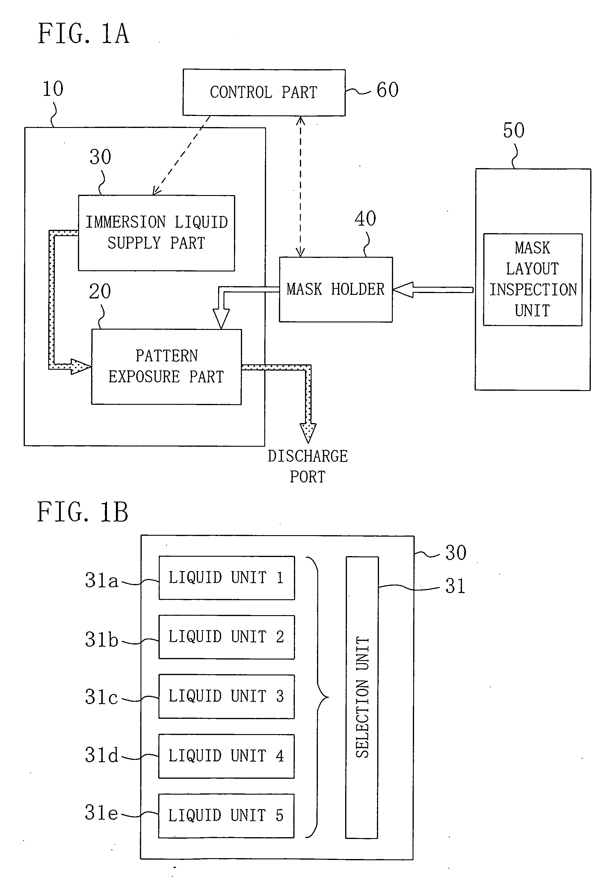
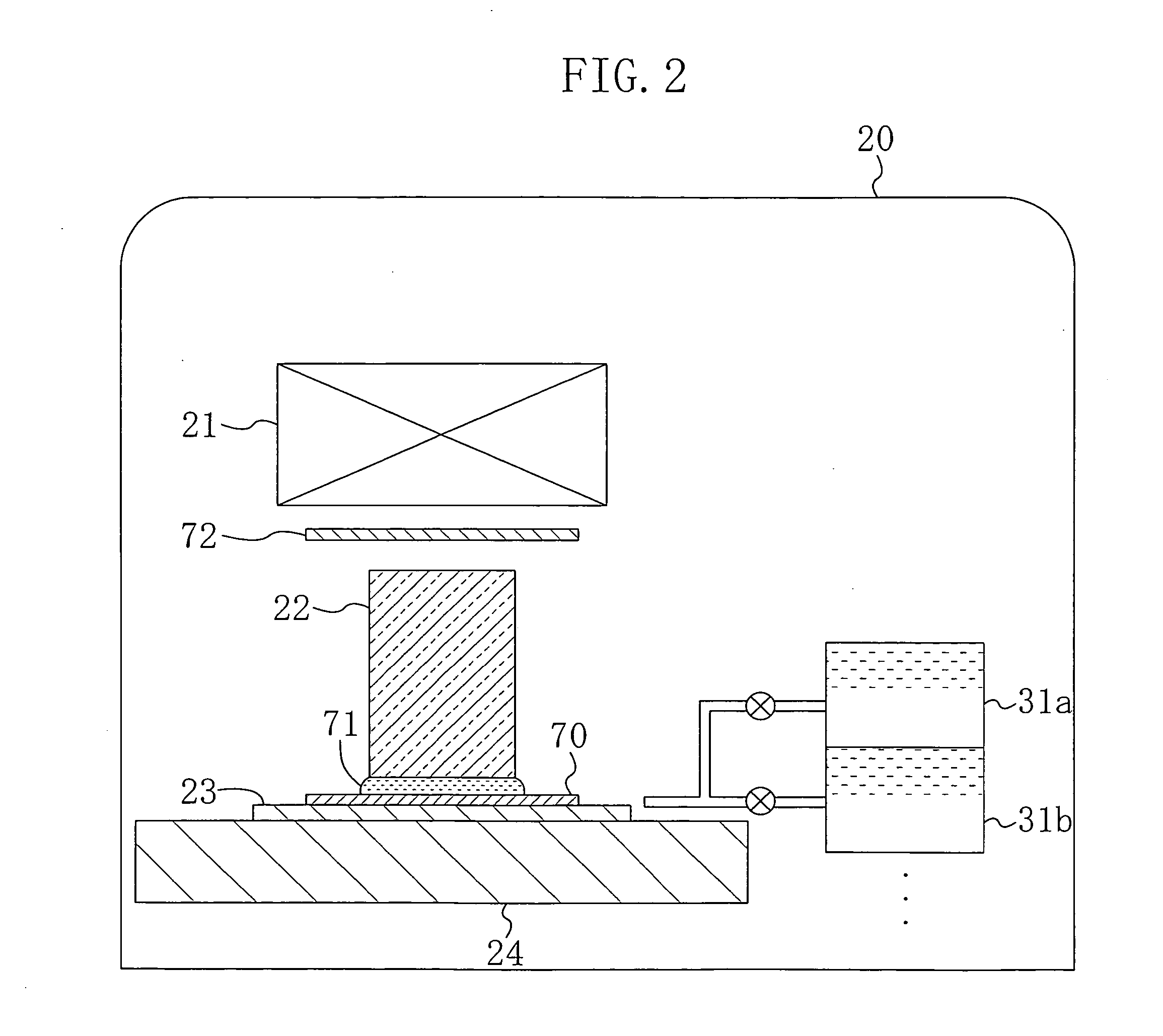
[0054]FIG. 1A schematically shows the system architecture of a semiconductor manufacturing apparatus employing immersion lithography according to Embodiment 1 of the invention, and FIG. 1B is a block diagram of an immersion liquid supply part of the semiconductor manufacturing apparatus.

[0055] As shown in FIG. 1A, the semiconductor manufacturing apparatus 10 of the invention includes a pattern exposure part 20 for performing pattern exposure on a resist film formed on a wafer; an immersion liquid supply part 30 for supplying an immersion liquid to the pattern exposure part 20; and a control part 60 for determining a pattern of a mask (reticle) to be used.

[0056] A mask holder 40 for temporarily storing a plurality of masks respectively having design patterns transports a mask to be used in exposure to the pattern exposure part 20. Each mask is subjected to a predetermined inspect...

embodiment 2

[0071] Now, a method for fabricating a semiconductor device (pattern formation method) according to Embodiment 2 using the semiconductor manufacturing apparatus of the invention will be described with reference to FIGS. 5A through 5D, 6A through 6D and 7A through 7D.

[0072] First, a positive chemically amplified resist material having the following composition is prepared:

Base polymer: poly((norbornene-5-methylene-t-butylcarboxylate) (50 mol %) -   2 g(maleic anhydride) (50 mol %))Acid generator: triphenylsulfonium triflate 0.06 gQuencher: triethanolamine0.002 gSolvent: propylene glycol monomethyl ether acetate  20 g

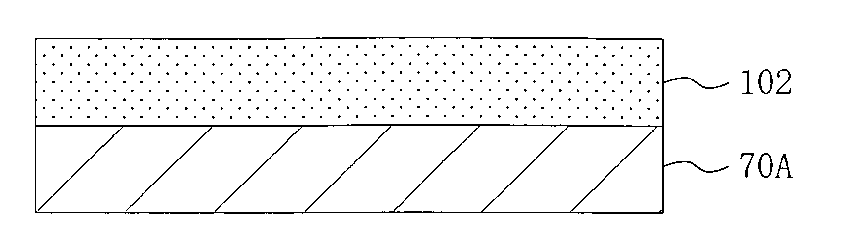
[0073] Next, as shown in FIG. 5A, the aforementioned chemically amplified resist material is applied on a substrate 70A so as to form a resist film 102 with a thickness of 0.35 μm.

[0074] Then, as shown in FIG. 5B, a first immersion liquid 71A of water having a refractive index of 1.44 is provided between the resist film 102 and a projection lens 22. Under this conditi...

embodiment 3

[0083] A method for fabricating a semiconductor device according to Embodiment 3 using the semiconductor manufacturing apparatus of the invention will now be described.

[0084] For providing different refractive indexes to immersion liquids, the compositions of additives in the respective immersion liquids are different in Embodiment 2. In contrast, the same additive is used but its content is changed so as to change the refractive index of an immersion liquid in Embodiment 3. Therefore, immersion liquids having various refractive indexes can be supplied without preparing a plurality of immersion liquids having different compositions.

[0085] In particular, when the content of the additive of a liquid is controlled, immersion liquids having a small difference in the refractive index can be supplied. Therefore, this embodiment is useful when the refractive index is desired to be adjusted in a minute range.

[0086] Accordingly, in the case where pattern widths and layouts are largely dif...


PUM

PropertyMeasurementUnit
thicknessaaaaaaaaaa
refractive indexaaaaaaaaaa

Abstract

An exposure system includes an exposure part for irradiating a resist film formed on a substrate with exposing light through a mask with a liquid provided on the resist film; and a liquid supply part for supplying the liquid to the exposure part. The liquid supplying part includes a plurality of liquid units respectively containing a plurality of liquids having different refractive indexes, and a selection unit for selecting one liquid unit from the plural liquid units and supplying a liquid contained in the selected liquid unit to the exposure part.

Description

CROSS-REFERENCE TO RELATED APPLICATIONS [0001] This application claims priority under 35 U.S.C. §119 on Patent Application No. 2004-212839 filed in Japan on Jul. 21, 2004, the entire contents of which are hereby incorporated by reference. BACKGROUND OF THE INVENTION [0002] The present invention relates to an exposure system, an exposure method and a method for fabricating a semiconductor device for immersion exposure for use in fabrication process or the like for semiconductor devices. [0003] In accordance with the increased degree of integration of semiconductor integrated circuits and downsizing of semiconductor devices, there are increasing demands for further rapid development of lithography technique. Currently, pattern formation is carried out through photolithography using exposing light of a mercury lamp, KrF excimer laser, ArF excimer laser or the like, and use of F2 laser lasing at a shorter wavelength is being examined. However, since there remain a large number of proble...

Claims


Application Information

Patent Timeline
Patent Type & Authority Applications(United States)
IPC IPC(8): G03B27/00G03F7/20
CPCG03F7/70341G03F7/2041
Inventor ENDO, MASAYUKISASAGO, MASARU
Owner PANASONIC CORP
Why Eureka
Try Eureka