

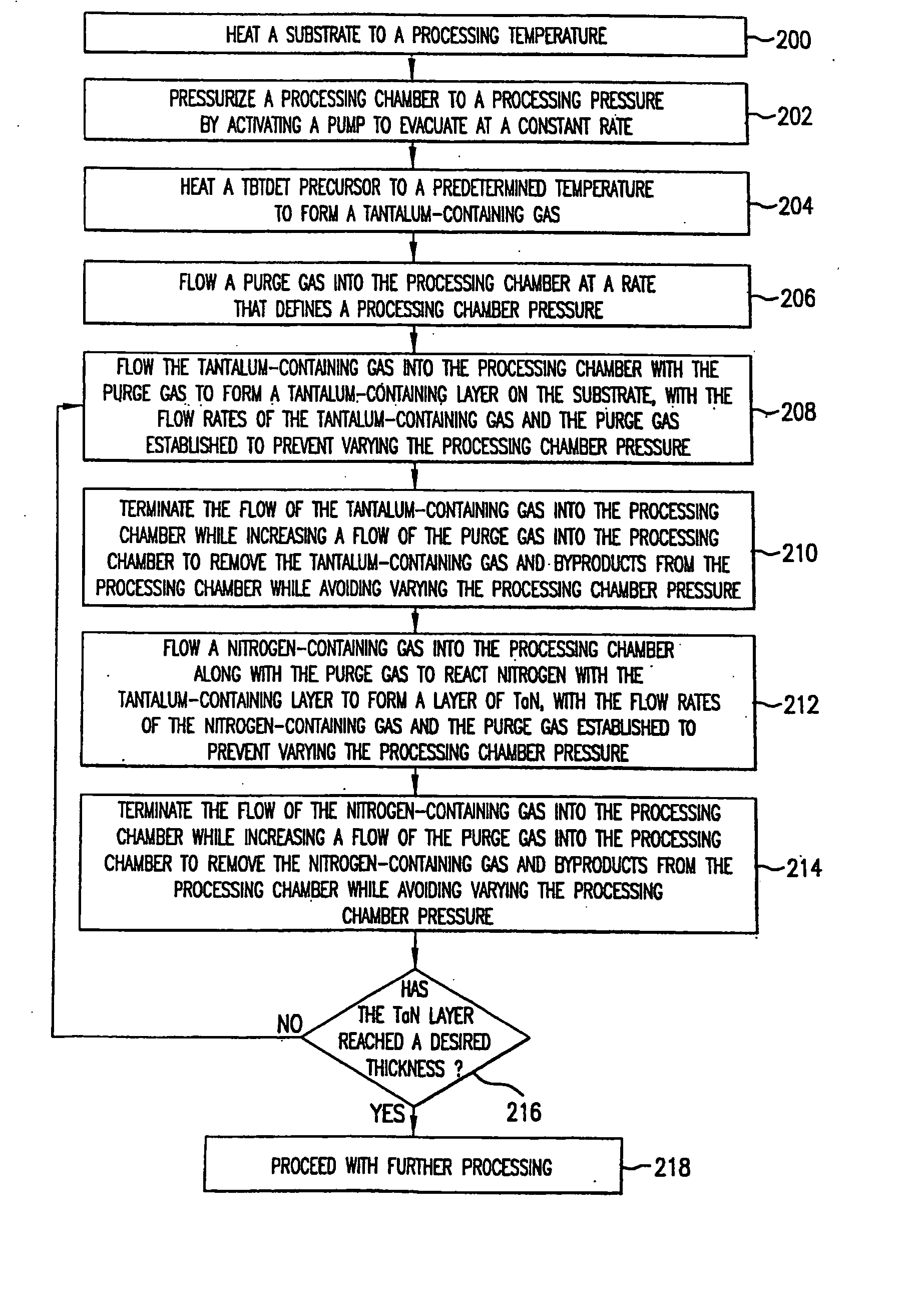
Sequential deposition of tantalum nitride using a tantalum-containing precursor and a nitrogen-containing precursor
a technology of tantalum nitride and precursor, which is applied in the field of sequential deposition of tantalum nitride using a tantalum-containing precursor and a nitrogen-containing precursor, can solve the problems of limited use of tantalum and/or tantalum nitride films, failure to increase the operational frequency of integrated circuits, and undesirable intermetallic alloys
- Summary
- Abstract
- Description
- Claims
- Application Information
AI Technical Summary
Benefits of technology
Problems solved by technology
Method used
Image

Examples
Embodiment Construction
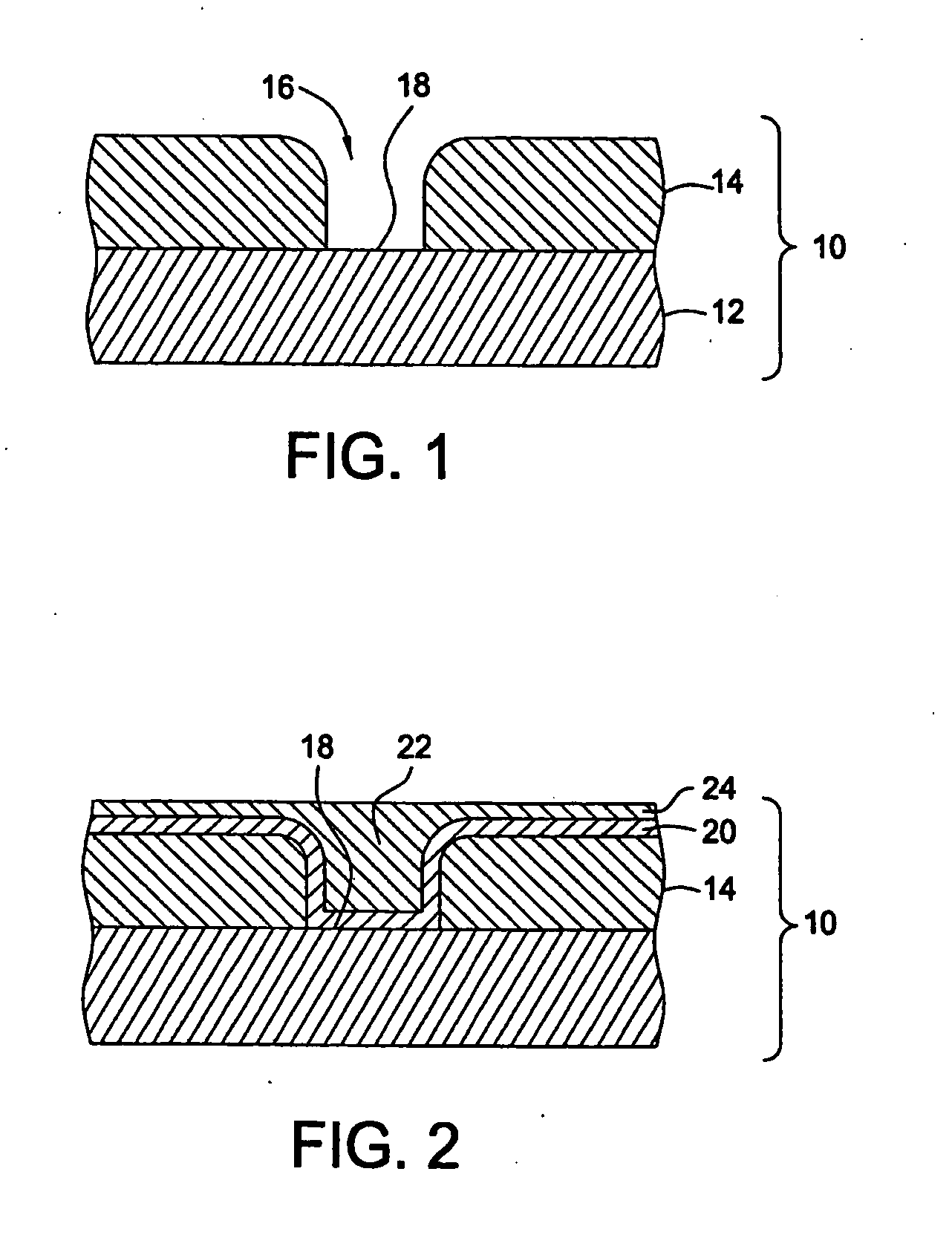
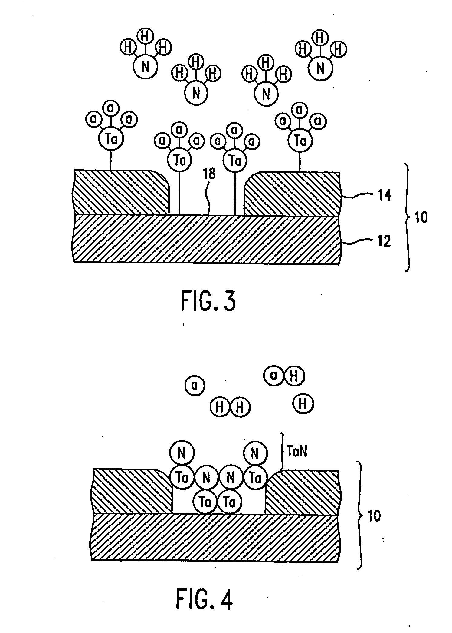
[0024] Referring to FIG. 1 an exemplary structure upon which a tantalum nitride layer, discussed more fully below, is formed in accordance with the present invention is shown as a substrate 10. Substrate 10 includes a wafer 12 that may have one or more layers, shown as layer 14, disposed thereon. Wafer 12 may be formed from any material suitable for semiconductor processing, such as silicon, and layer 14 may be formed from any suitable material, including dielectric or conductive materials. For purposes of the present example, layer 14 includes a void 16, exposing a region 18 of wafer 12.
[0025] Embodiments of the processes described herein deposit tantalum-containing materials or tantalum nitride on many substrates and surfaces. Substrates on which embodiments of the invention may be useful include, but are not limited to semiconductor wafers, such as crystalline silicon (e.g., Si or Si), silicon oxide, silicon germanium, doped or undoped polysilicon, doped or undoped silicon wafer...
PUM
| Property | Measurement | Unit |
|---|---|---|
| temperature | aaaaa | aaaaa |
| temperature | aaaaa | aaaaa |
| sizes | aaaaa | aaaaa |
Abstract
Description
Claims
Application Information